


Part Number: TMS570LS1227
Hi,
I have TMS570LS1227 HDK that i am using with the I2C slave chip. The master i2c configuration is as below.
/** - set i2c mode */
i2cREG1->MDR = (uint32)((uint32)0U << 15U) /* nack mode */
| (uint32)((uint32)0U << 14U) /* free running */
| (uint32)(0U) /* start condition - master only */
| (uint32)((uint32)1U <<11U) /* stop condition */
| (uint32)((uint32)1U <<10U) /* Master/Slave mode */
| (uint32)((uint32)I2C_TRANSMITTER) /* Transmitter/receiver */
| (uint32)((uint32)I2C_7BIT_AMODE) /* xpanded address */
| (uint32)((uint32)1U << 7U) /* repeat mode */
| (uint32)((uint32)0U << 6U) /* digital loop back */
| (uint32)((uint32)0U << 4U) /* start byte - master only */
| (uint32)((uint32)0U << 3U) /* free data format */
| (uint32)(I2C_8_BIT); /* bit count */
/** - set i2c Backward Compatibility mode */
i2cREG1->EMDR = 0U;
/** - Disable DMA */
i2cREG1->DMACR = 0x00U;
/** - set i2c data count */
i2cREG1->CNT = 8U;
/** - disable all interrupts */
i2cREG1->IMR = 0x00U;
/** - set prescale */
i2cREG1->PSC = 10U;
/** - set clock rate */
i2cREG1->CKH = 36U;
i2cREG1->CKL = 36U;
/** - set i2c pins functional mode */
i2cREG1->PFNC = (1U);
/** - set i2c pins default output value */
i2cREG1->DOUT = (uint32)((uint32)1U << 1U) /* sda pin */
| (uint32)(1U); /* scl pin */
/** - set i2c pins output direction */
i2cREG1->DIR = (uint32)((uint32)1U << 1U) /* sda pin */
| (uint32)(1U); /* scl pin */
/** - set i2c pins open drain enable */
i2cREG1->PDR = (uint32)((uint32)1U << 1U) /* sda pin */
| (uint32)(1U); /* scl pin */
/** - set i2c pins pullup/pulldown enable */
i2cREG1->PDIS = (uint32)((uint32)0U << 1U) /* sda pin */
| (uint32)(0U); /* scl pin */
/** - set i2c pins pullup/pulldown select */
i2cREG1->PSEL = (uint32)((uint32)1U << 1U) /* sda pin */
| (uint32)(1U); /* scl pin */
It works perfectly alright. However, there are some instances the slave need more time to process the request. The slave i2c data sheet explains
"the i2c chip requires execution time while it runs each instruction. An external master can get a successful result after this time has elapsed. If the external master sends a read instruction in the middle of an unfinished execution it will receive the error (0xFF) of 1byte.".
The properly working sequence is as below. In this table as i mentioned in the third column, the slave respond NAK for the read followed by 0xFF + ACK, reread -> NAK, 0xFF +ACK...until it will respond with ACK for the read.
| Time [s] | Analyzer Name | Decoded Protocol Result | |
| 0.24614475 | I2C | Setup Read to [0xC9] + ACK | |
| 0.246235625 | I2C | 0x04 + ACK | |
| 0.246334 | I2C | 0x11 + ACK | |
| 0.24643725 | I2C | 0x33 + ACK | |
| 0.246543 | I2C | 0x43 + NAK | |
| 0.250027375 | I2C | Setup Write to [0xC8] + ACK | 1st write to request slave |
| 0.25011825 | I2C | 0x03 + ACK | |
| 0.2502115 | I2C | 0x27 + ACK | |
| 0.25030475 | I2C | 0x81 + ACK | |
| 0.250400625 | I2C | 0x04 + ACK | |
| 0.250498875 | I2C | 0x00 + ACK | |
| 0.25059975 | I2C | 0x00 + ACK | |
| 0.250698 | I2C | 0x8E + ACK | |
| 0.250796375 | I2C | 0x54 + ACK | |
| 0.250892125 | I2C | 0x00 + ACK | |
| 0.250990375 | I2C | 0x00 + ACK | |
| 0.25108875 | I2C | 0x00 + ACK | |
| 0.2511845 | I2C | 0x00 + ACK | |
| 0.251282875 | I2C | 0x00 + ACK | |
| 0.25138125 | I2C | 0x00 + ACK | |
| 0.251477 | I2C | 0x0E + ACK | |
| 0.25157775 | I2C | 0x54 + ACK | |
| 0.251676125 | I2C | 0x00 + ACK | |
| 0.251774375 | I2C | 0x00 + ACK | |
| 0.25187025 | I2C | 0x00 + ACK | |
| 0.2519685 | I2C | 0x00 + ACK | |
| 0.25206675 | I2C | 0x00 + ACK | |
| 0.252162625 | I2C | 0x00 + ACK | |
| 0.252260875 | I2C | 0x0E + ACK | |
| 0.252359125 | I2C | 0x54 + ACK | |
| 0.252455 | I2C | 0x00 + ACK | |
| 0.25255325 | I2C | 0x00 + ACK | |
| 0.252654 | I2C | 0x00 + ACK | |
| 0.252752375 | I2C | 0x00 + ACK | |
| 0.25284825 | I2C | 0x00 + ACK | |
| 0.2529465 | I2C | 0x00 + ACK | |
| 0.25304475 | I2C | 0x0E + ACK | |
| 0.253140625 | I2C | 0x54 + ACK | |
| 0.253238875 | I2C | 0x00 + ACK | |
| 0.25333725 | I2C | 0x00 + ACK | |
| 0.253433 | I2C | 0x00 + ACK | |
| 0.253531375 | I2C | 0x00 + ACK | |
| 0.253632125 | I2C | 0x00 + ACK | |
| 0.2537305 | I2C | 0x00 + ACK | |
| 0.25382875 | I2C | 0x46 + ACK | |
| 0.253924625 | I2C | 0x64 + ACK | |
| 0.2540505 | I2C | Setup Read to [0xC9] + NAK | 1st Read to slave for the result |
| 0.25414125 | I2C | 0xFF + ACK | |
| 0.25725775 | I2C | Setup Read to [0xC9] + NAK | |
| 0.2573485 | I2C | 0xFF + ACK | |
| 0.26026525 | I2C | Setup Read to [0xC9] + NAK | |
| 0.260356 | I2C | 0xFF + ACK | |
| 0.2632345 | I2C | Setup Read to [0xC9] + NAK | |
| 0.26332525 | I2C | 0xFF + ACK | |
| 0.266262625 | I2C | Setup Read to [0xC9] + NAK | |
| 0.2663535 | I2C | 0xFF + ACK | |
| 0.269270125 | I2C | Setup Read to [0xC9] + NAK | |
| 0.269361 | I2C | 0xFF + ACK | |
| 0.272236375 | I2C | Setup Read to [0xC9] + NAK | |
| 0.272327125 | I2C | 0xFF + ACK | |
| 0.275285125 | I2C | Setup Read to [0xC9] + NAK | |
| 0.275376 | I2C | 0xFF + ACK | |
| 0.278275125 | I2C | Setup Read to [0xC9] + NAK | |
| 0.278365875 | I2C | 0xFF + ACK | |
| 0.281220625 | I2C | Setup Read to [0xC9] + NAK | |
| 0.281311375 | I2C | 0xFF + ACK | |
| 0.28424875 | I2C | Setup Read to [0xC9] + NAK | |
| 0.2843395 | I2C | 0xFF + ACK | |
| 0.28725625 | I2C | Setup Read to [0xC9] + ACK | Slave respond successfully |
| 0.287347125 | I2C | 0x04 + ACK | |
| 0.2878655 | I2C | 0x00 + ACK | |
| 0.287966375 | I2C | 0x03 + ACK | |
| 0.28807225 | I2C | 0x40 + NAK | |
| 0.289808625 | I2C | Setup Write to [0xC8] + ACK | 2nd Write to request slave |
| 0.289899375 | I2C | 0x03 + ACK | |
| 0.289992625 | I2C | 0x27 + ACK | |
| 0.290091 | I2C | 0x81 + ACK | |
| 0.29018675 | I2C | 0x00 + ACK | |
| 0.290285 | I2C | 0x00 + ACK | |
| 0.29038325 | I2C | 0x01 + ACK | |
| 0.290479125 | I2C | 0x04 + ACK | |
| 0.290577375 | I2C | 0x05 + ACK | |
| 0.290675625 | I2C | 0x05 + ACK | |
| 0.290771375 | I2C | 0x05 + ACK | |
| 0.29087225 | I2C | 0x11 + ACK | |
| 0.2909705 | I2C | 0x22 + ACK | |
| 0.291068875 | I2C | 0x33 + ACK | |
| 0.291164625 | I2C | 0x44 + ACK | |
| 0.291262875 | I2C | 0x00 + ACK | |
| 0.29136125 | I2C | 0x00 + ACK | |
| 0.291457 | I2C | 0x00 + ACK | |
| 0.29155525 | I2C | 0x00 + ACK | |
| 0.291653625 | I2C | 0x00 + ACK | |
| 0.2917495 | I2C | 0x00 + ACK | |
| 0.29185275 | I2C | 0x00 + ACK | |
| 0.2919485 | I2C | 0x00 + ACK | |
| 0.292046875 | I2C | 0x00 + ACK | |
| 0.29214275 | I2C | 0x00 + ACK | |
| 0.292241 | I2C | 0x00 + ACK | |
| 0.29233925 | I2C | 0x00 + ACK | |
| 0.292435125 | I2C | 0x00 + ACK | |
| 0.292533375 | I2C | 0x00 + ACK | |
| 0.29263175 | I2C | 0x00 + ACK | |
| 0.2927275 | I2C | 0x00 + ACK | |
| 0.29283075 | I2C | 0x00 + ACK | |
| 0.292929125 | I2C | 0x00 + ACK | |
| 0.2930275 | I2C | 0x00 + ACK | |
| 0.29312575 | I2C | 0x00 + ACK | |
| 0.2932215 | I2C | 0x00 + ACK | |
| 0.293319875 | I2C | 0x00 + ACK | |
| 0.29341825 | I2C | 0x00 + ACK | |
| 0.293514 | I2C | 0x00 + ACK | |
| 0.29361225 | I2C | 0x02 + ACK | |
| 0.2937105 | I2C | 0x3B + ACK | |
| 0.2938365 | I2C | Setup Read to [0xC9] + NAK | 2nd read to slave results |
| 0.29392725 | I2C | 0xFF + ACK | |
| 0.297190875 | I2C | Setup Read to [0xC9] + NAK | |
| 0.29728175 | I2C | 0xFF + ACK | |
| 0.300219125 | I2C | Setup Read to [0xC9] + NAK | |
| 0.300309875 | I2C | 0xFF + ACK | |
| 0.303226625 | I2C | Setup Read to [0xC9] + NAK | |
| 0.303317375 | I2C | 0xFF + ACK | |
| 0.306213375 | I2C | Setup Read to [0xC9] + NAK | |
| 0.30630425 | I2C | 0xFF + ACK | |
| 0.309162 | I2C | Setup Read to [0xC9] + NAK | |
| 0.30925275 | I2C | 0xFF + ACK | |
| 0.3121695 | I2C | Setup Read to [0xC9] + NAK | |
| 0.31226025 | I2C | 0xFF + ACK | |
| 0.315363 | I2C | Setup Read to [0xC9] + NAK | |
| 0.315453875 | I2C | 0xFF + ACK | |
| 0.31913925 | I2C | Setup Read to [0xC9] + NAK | |
| 0.31923 | I2C | 0xFF + ACK | |
| 0.32214675 | I2C | Setup Read to [0xC9] + NAK | |
| 0.3222375 | I2C | 0xFF + ACK | |
| 0.32509525 | I2C | Setup Read to [0xC9] + NAK | |
| 0.325186 | I2C | 0xFF + ACK | |
| 0.32816475 | I2C | Setup Read to [0xC9] + ACK | successful slave result |
| 0.328255625 | I2C | 0x04 + ACK | |
| 0.328811625 | I2C | 0x00 + ACK | |
| 0.328912375 | I2C | 0x03 + ACK | |
| 0.32902075 | I2C | 0x40 + NAK | |
| 0.3336655 | I2C | Setup Write to [0xC8] + ACK | |
| 0.33375625 | I2C | 0x03 + ACK | |
| 0.333849625 | I2C | 0x0B + ACK | |
| 0.333942875 | I2C | 0x82 + ACK | |
| 0.334043625 | I2C | 0x00 + ACK | |
| 0.3341395 | I2C | 0x00 + ACK | |
| 0.33423775 | I2C | 0x00 + ACK | |
| 0.334336 | I2C | 0x11 + ACK | |
| 0.334431875 | I2C | 0x22 + ACK | |
| 0.334530125 | I2C | 0x33 + ACK | |
| 0.334628375 | I2C | 0x44 + ACK | |
| 0.33472425 | I2C | 0x3E + ACK | |
| 0.3348225 | I2C | 0xD2 + ACK | |
| 0.334948375 | I2C | Setup Read to [0xC9] + NAK | |
| 0.335039125 | I2C | 0xFF + ACK | |
| 0.338117375 | I2C | Setup Read to [0xC9] + NAK | |
| 0.33820825 | I2C | 0xFF + ACK | |
| 0.341062875 | I2C | Setup Read to [0xC9] + NAK | |
| 0.34115375 | I2C | 0xFF + ACK | |
| 0.344049 | I2C | Setup Read to [0xC9] + NAK | |
| 0.344139875 | I2C | 0xFF + ACK | |
| 0.3470565 | I2C | Setup Read to [0xC9] + NAK | |
| 0.347147375 | I2C | 0xFF + ACK | |
| 0.350398625 | I2C | Setup Read to [0xC9] + NAK | |
| 0.350489375 | I2C | 0xFF + ACK | |
| 0.353406125 | I2C | Setup Read to [0xC9] + NAK | |
| 0.353496875 | I2C | 0xFF + ACK | |
| 0.35649625 | I2C | Setup Read to [0xC9] + NAK | |
| 0.356587125 | I2C | 0xFF + ACK | |
| 0.359589625 | I2C | Setup Read to [0xC9] + NAK | |
| 0.359680375 | I2C | 0xFF + ACK | |
| 0.362535125 | I2C | Setup Read to [0xC9] + NAK | |
| 0.362625875 | I2C | 0xFF + ACK | |
| 0.36610075 | I2C | Setup Read to [0xC9] + NAK | |
| 0.3661915 | I2C | 0xFF + ACK | |
| 0.36919475 | I2C | Setup Read to [0xC9] + NAK | |
| 0.3692855 | I2C | 0xFF + ACK | |
| 0.372450375 | I2C | Setup Read to [0xC9] + NAK | |
| 0.372541125 | I2C | 0xFF + ACK | |
| 0.37531625 | I2C | Setup Read to [0xC9] + NAK | |
| 0.375407 | I2C | 0xFF + ACK | |
| 0.378344375 | I2C | Setup Read to [0xC9] + NAK | |
| 0.378435125 | I2C | 0xFF + ACK | |
| 0.3812485 | I2C | Setup Read to [0xC9] + NAK | |
| 0.38133925 | I2C | 0xFF + ACK | |
| 0.384442125 | I2C | Setup Read to [0xC9] + NAK | |
| 0.384532875 | I2C | 0xFF + ACK | |
| 0.387490875 | I2C | Setup Read to [0xC9] + NAK | |
| 0.38758175 | I2C | 0xFF + ACK | |
| 0.390460125 | I2C | Setup Read to [0xC9] + NAK | |
| 0.390551 | I2C | 0xFF + ACK | |
| 0.393736375 | I2C | Setup Read to [0xC9] + NAK | |
| 0.393827125 | I2C | 0xFF + ACK | |
| 0.39659925 | I2C | Setup Read to [0xC9] + NAK | |
| 0.39669 | I2C | 0xFF + ACK | |
| 0.39966875 | I2C | Setup Read to [0xC9] + ACK | successful result |
| 0.399759625 | I2C | 0x04 + ACK | |
| 0.4003205 | I2C | 0x00 + ACK | |
| 0.400421375 | I2C | 0x03 + ACK | |
| 0.400524625 | I2C | 0x40 + NAK |
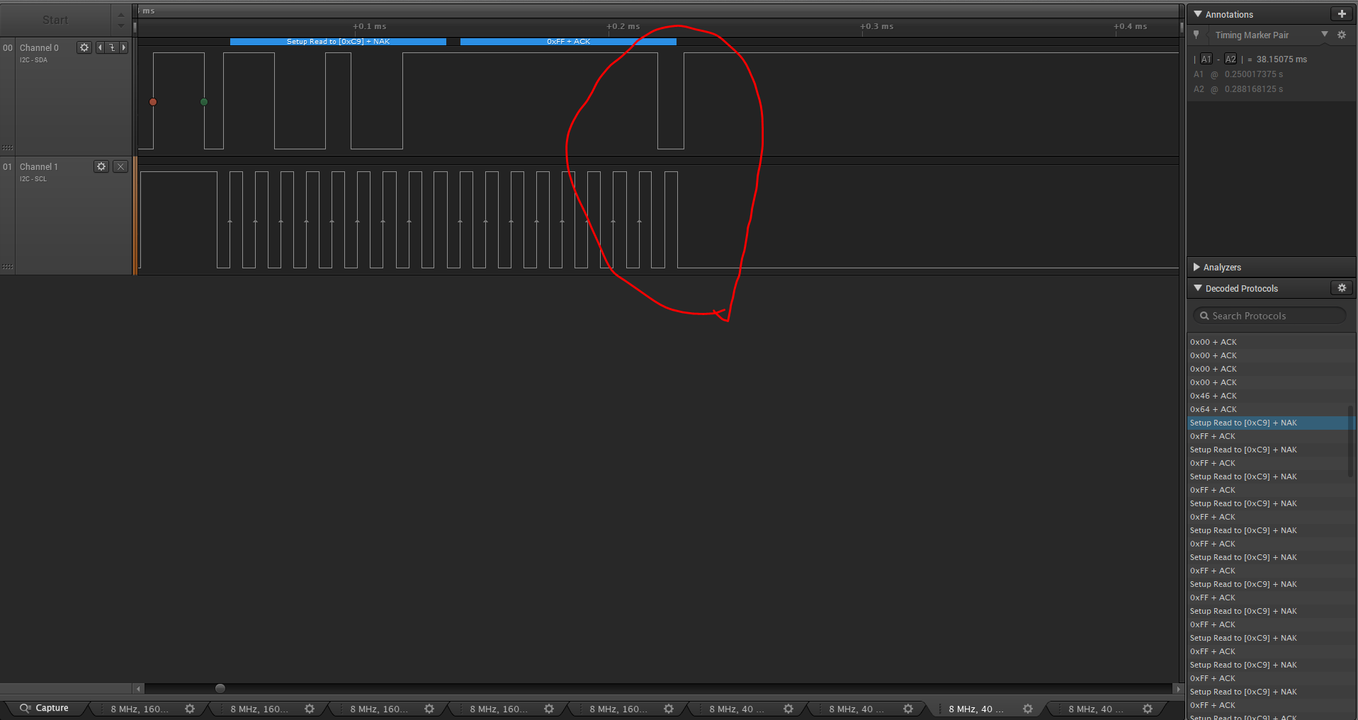
If i try to implement this in TMS570LS12x, the master pull down the SCL line as soon as the slave responds NAK for the read. setting the ignore NACK in EMDR doesnt help as it just continue read and copy the data as 0xFF for 4 times as the counts set to 4.
In the above picture once the slave respond NAK for the read and 0xFF+ACK, the SCL is held for ~3millisec and re read the slave and continues...
How do we recover the TMS570LS12x master once it stuck with NAK response from slave and to implement the above fucntions?
Could you please help me to implement this in TMS570LS12x controller?
Thanks,
Best Regards,
-Dinesh
