Other Parts Discussed in Thread: MSP430F5529
Hi All,
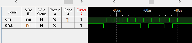
I have been trying to implement bit-banged I2C communication protocol on TM4C123GH6PM. My problem is, I am not able to figure-out the right configuration for the GPIO registers in order to get the I2C working in right way. Can you please help me in this regard?
Pins being used for I2C:
Pin PF1 - SDA
Pin PF2 - SCL
Slave device - MSP430F5529 (It uses Hardware I2C)
Master device - TM4C123GH6PM (It uses Software (bitbanged) I2C)
External pull-up resistors for SDA & SCL - 10 KOhm each
The functions written for I2C are,
/* Configure I2C */
void I2C_Configure(void)
{
/* GPIO Initialization and Configuration */
SYSCTL->GPIOHBCTL_b.PORTF = 0; SYSCTL->RCGCGPIO_b.PORTF = 1;
/* Enable Clock to the GPIO Modules (SYSCTL->RCGCGPIO) */
SYSCTL->RCGCGPIO |= 0x20; /* Port F */
/* Allow time for clock to stabilize (SYSCTL->PRGPIO) */
while((SYSCTL->PRGPIO & (0x20) ) != (0x20) ){};
// 3. Set Analog Mode Select bits for each Port (GPIO->AMSEL 0=digital, 1=analog)
GPIOF->AMSEL = 0x00;
// 4. Set Port Control Register for each Port (GPIO->PCTL, check the PCTL table)
GPIOF->PCTL = 0x00;
// 5. Set Alternate Function Select bits for each Port (GPIO->AFSEL 0=regular I/O, 1=PCTL peripheral)
GPIOF->AFSEL = 0x00;
// 6. Set Output pins for each Port (Direction of the Pins: GPIO->DIR 0=input, 1=output)
GPIOF->DIR = ~(I2C_SDA | I2C_SCL); // PF2,PF1 for Input
// 8. Set Digital Enable register on all GPIO pins (GPIO->DEN 0=disable, 1=enable)
GPIOF->DEN = I2C_SDA | I2C_SCL; // Enable all digital pins on PortF (PF2,PF1)
/* Set DATA register as 0 always for SDA and SCL */
GPIOF->DATA = ~(I2C_SDA | I2C_SCL);
GPIOF->ODR = I2C_SDA | I2C_SCL;
I2C_SCL_HIGH();
I2C_SDA_HIGH();
/* Small delay */
xdelay(I2C_DELAY_VALUE);
}
/* SDA HIGH */
void I2C_SDA_HIGH(void)
{
/* Data enable disabled to float SDA */
GPIOF->DIR &= ~I2C_SDA;
//GPIOF->ODR &= ~I2C_SDA;
/* Small delay */
xdelay(I2C_DELAY_VALUE);
}
/* SDA LOW */
void I2C_SDA_LOW(void)
{
/* Output */
GPIOF->DIR |= I2C_SDA;
//GPIOF->ODR |= I2C_SDA;
/* Small delay */
xdelay(I2C_DELAY_VALUE);
}
/* SCL HIGH */
void I2C_SCL_HIGH(void)
{
/* Data enable disabled to float SCL */
GPIOF->DIR &= ~I2C_SCL;
//GPIOF->ODR &= ~I2C_SCL;
/* Small delay */
xdelay(I2C_DELAY_VALUE<<1);
}
/* SCL LOW */
void I2C_SCL_LOW(void)
{
/* Output */
GPIOF->DIR |= I2C_SCL;
//GPIOF->ODR |= I2C_SCL;
/* Small delay */
xdelay(I2C_DELAY_VALUE);
}
Are the four functions I2C_SCL_LOW, I2C_SCL_HIGH, I2C_SDA_HIGH and I2C_SDA_LOW are safe to use or have the right configuration when the external pull-up used?
Note: I have already done similar implementation in MSP430 MCU, but I wanted to switch to TIVA series.
Thanks in advAnce,
vksalian