


Part Number: TMS570LS3137
Tool/software: Code Composer Studio
After the configuration of TMS570LS31 SCI mode of LIN-DMA(131/132pin), if the delay is increased, a garble code will be sent; if the delay is deleted, it will be sent normally.May I ask what causes it?
Software configuration is as follows:
sciBASE_t* uartREG[2] = {sciREG,scilinREG};
/*
* @Brief:
* uart initialization
* @ Param:
* uartx: serial number, 0 or 1
* buad_rate: serial port baud rate
* Parity: (-1 without parity, 0-even, 1-parity)
*/
void bsp_uart_open(uint8 uartx, uint32 buad_rate,sint8 parity)
{
uint8 parEn = parity == -1 ? 0 : 1;
uint8 parVal = parity == 1 ? 0 : 1;
uartx &= 0x3;
/** initialize SCI */
uartREG[uartx]->GCR1 &= ~0x80U;
/** - bring SCI out of reset */
uartREG[uartx]->GCR0 = 0U;
uartREG[uartx]->GCR0 = 1U;
/** - Disable all interrupts */
uartREG[uartx]->CLEARINT = 0xFFFFFFFFU;
uartREG[uartx]->CLEARINTLVL = 0xFFFFFFFFU;
/** - global control 1 */
uartREG[uartx]->GCR1 = (uint32)((uint32)1U << 25U) /* enable transmit */
| (uint32)((uint32)1U << 24U) /* enable receive */
| (uint32)((uint32)1U << 5U) /* internal clock (device has no clock pin) */
| (uint32)((uint32)0U << 4U) /* number of stop bits */
| (uint32)((uint32)parVal << 3U) /* even parity, otherwise odd */
| (uint32)((uint32)parEn << 2U) /* enable parity */
| (uint32)((uint32)1U << 1U); /* asynchronous timing mode */
/** - set baudrate */
uartREG[uartx]->BRS = buad_rate; /* baudrate */
/** - transmission length */
uartREG[uartx]->FORMAT = 8U - 1U; /* length */
/** - set SCI pins functional mode */
uartREG[uartx]->PIO0 = (uint32)((uint32)1U << 2U) /* tx pin */
| (uint32)((uint32)1U << 1U); /* rx pin */
/** - set SCI pins default output value */
uartREG[uartx]->PIO3 = (uint32)((uint32)0U << 2U) /* tx pin */
| (uint32)((uint32)0U << 1U); /* rx pin */
/** - set SCI pins output direction */
uartREG[uartx]->PIO1 = (uint32)((uint32)1U << 2U) /* tx pin */
| (uint32)((uint32)0U << 1U); /* rx pin */
/** - set SCI pins open drain enable */
uartREG[uartx]->PIO6 = (uint32)((uint32)0U << 2U) /* tx pin */
| (uint32)((uint32)0U << 1U); /* rx pin */
/** - set SCI pins pullup/pulldown enable */
uartREG[uartx]->PIO7 = (uint32)((uint32)0U << 2U) /* tx pin */
| (uint32)((uint32)0U << 1U); /* rx pin */
/** - set SCI pins pullup/pulldown select */
uartREG[uartx]->PIO8 = (uint32)((uint32)1U << 2U) /* tx pin */
| (uint32)((uint32)1U << 1U); /* rx pin */
/** - set interrupt level */
uartREG[uartx]->SETINTLVL = (uint32)((uint32)0U << 26U) /* Framing error */
| (uint32)((uint32)0U << 25U) /* Overrun error */
| (uint32)((uint32)0U << 24U) /* Parity error */
| (uint32)((uint32)0U << 9U) /* Receive */
| (uint32)((uint32)0U << 8U) /* Transmit */
| (uint32)((uint32)0U << 1U) /* Wakeup */
| (uint32)((uint32)0U << 0U); /* Break detect */
/** - set interrupt enable */
uartREG[uartx]->SETINT = (uint32)((uint32)0U << 26U) /* Framing error */
| (uint32)((uint32)0U << 25U) /* Overrun error */
| (uint32)((uint32)0U << 24U) /* Parity error */
| (uint32)((uint32)0U << 9U) /* 1 Receive */
| (uint32)((uint32)0U << 1U) /* Wakeup */
| (uint32)((uint32)0U << 0U); /* Break detect */
/** - initialize global transfer variables */
g_sciTransfer_t[uartx].mode = (uint32)0U << 8U;
g_sciTransfer_t[uartx].tx_length = 0U;
g_sciTransfer_t[uartx].rx_length = 0;
/** - Finaly start SCI */
uartREG[uartx]->GCR1 |= 0x80U;
}
#define SCI_TX_ADDR ((uint32_t)(&(uartREG[0]->TD)) + 3)
#define SCI_RX_ADDR ((uint32_t)(&(uartREG[0]->RD)) + 3)
#define LIN_TX_ADDR ((uint32_t)(&(uartREG[1]->TD)) + 3)
#define LIN_RX_ADDR ((uint32_t)(&(uartREG[1]->RD)) + 3)
#define DMA_SCI_TX DMA_REQ31
#define DMA_SCI_RX DMA_REQ30
#define DMA_LIN_TX DMA_REQ29
#define DMA_LIN_RX DMA_REQ28
#define SCI_SET_TX_DMA (1<<16)
#define SCI_SET_RX_DMA (1<<17)
#define SCI_SET_RX_DMA_ALL (1<<18)
void bsp_dma_enable (uint8 uartx,uint8 *txData,uint16 txSize,uint16 tx_CHx,uint8 *rxData,uint16 rxSize,uint16 rx_CHx);
uint8_t bsp_dma_send_data(uint16_t txSize,uint16 tx_CHx);
uint32_t bsp_dma_get_data(uint8_t *rxData,uint16 rxSize,uint16 rx_CHx);
void bsp_dma_enable (uint8 uartx,uint8 *txData,uint16 txSize,uint16 tx_CHx,uint8 *rxData,uint16 rxSize,uint16 rx_CHx)
{
uint32_t sciTxData, sciRxData;
g_dmaCTRL g_dmaCTRLPKT1, g_dmaCTRLPKT2;
while (((uartREG[uartx]->FLR & SCI_TX_INT) == 0U) || ((uartREG[uartx]->FLR & 0x4) == 0x4))
{
} /* Wait */
if(uartx == 0x0)
{
/*Assign DMA request SCI transmit to tx Channel x*/
dmaReqAssign(tx_CHx, DMA_SCI_TX);
/*Assign DMA request SCI receive to rx Channel x*/
dmaReqAssign(rx_CHx, DMA_SCI_RX);
}
else
{
/*Assign DMA request SCI transmit to tx Channel x*/
dmaReqAssign(tx_CHx, DMA_LIN_TX);
/*Assign DMA request SCI receive to rx Channel x*/
dmaReqAssign(rx_CHx, DMA_LIN_RX);
}
/* Addresses of SCI/LIN 8-bit TX/Rx data */
if(uartx == 0x0)
{
sciTxData = SCI_TX_ADDR;
sciRxData = SCI_RX_ADDR;
}
else
{
sciTxData = LIN_TX_ADDR;
sciRxData = LIN_RX_ADDR;
}
if(txSize > 0){
/*Configure control packet for tx Channel x*/
g_dmaCTRLPKT1.SADD = (uint32_t)txData; /* source address */
g_dmaCTRLPKT1.DADD = sciTxData; /* destination address */
g_dmaCTRLPKT1.CHCTRL = 0; /* channel control */
g_dmaCTRLPKT1.FRCNT = txSize; /* frame count */
g_dmaCTRLPKT1.ELCNT = 1; /* element count */
g_dmaCTRLPKT1.ELDOFFSET = 0; /* element destination offset */
g_dmaCTRLPKT1.ELSOFFSET = 0; /* element destination offset */
g_dmaCTRLPKT1.FRDOFFSET = 0; /* frame destination offset */
g_dmaCTRLPKT1.FRSOFFSET = 0; /* frame destination offset */
g_dmaCTRLPKT1.PORTASGN = 4; /* PORTB ONLY */
g_dmaCTRLPKT1.RDSIZE = ACCESS_8_BIT; /* read size */
g_dmaCTRLPKT1.WRSIZE = ACCESS_8_BIT; /* write size */
g_dmaCTRLPKT1.TTYPE = FRAME_TRANSFER; /* transfer type */
g_dmaCTRLPKT1.ADDMODERD = ADDR_INC1; /* address mode read */
g_dmaCTRLPKT1.ADDMODEWR = ADDR_FIXED; /* address mode write */
g_dmaCTRLPKT1.AUTOINIT = AUTOINIT_OFF; /* autoinit */
/*Set tx control packet for tx channel x*/
dmaSetCtrlPacket(tx_CHx, g_dmaCTRLPKT1);
/*Enable uartx Transmit DMA Request*/
uartREG[uartx]->SETINT |= SCI_SET_TX_DMA;
uartREG[uartx]->SETINT |= ((uint32_t)1<<8);
uartREG[uartx]->TD = 48;
}
if(rxSize > 0){
/*Configure control packet for Channel x*/
g_dmaCTRLPKT2.SADD = sciRxData; /* source address */
g_dmaCTRLPKT2.DADD = (uint32_t)rxData; /* destination address */
g_dmaCTRLPKT2.CHCTRL = 0; /* channel control */
g_dmaCTRLPKT2.FRCNT = rxSize; /* frame count */
g_dmaCTRLPKT2.ELCNT = 1; /* element count */
g_dmaCTRLPKT2.ELDOFFSET = 0; /* element destination offset */
g_dmaCTRLPKT2.ELSOFFSET = 0; /* element destination offset */
g_dmaCTRLPKT2.FRDOFFSET = 0; /* frame destination offset */
g_dmaCTRLPKT2.FRSOFFSET = 0; /* frame destination offset */
g_dmaCTRLPKT2.PORTASGN = 4; /* PORTB ONLY */
g_dmaCTRLPKT2.RDSIZE = ACCESS_8_BIT; /* read size */
g_dmaCTRLPKT2.WRSIZE = ACCESS_8_BIT; /* write size */
g_dmaCTRLPKT2.TTYPE = FRAME_TRANSFER; /* transfer type */
g_dmaCTRLPKT2.ADDMODERD = ADDR_FIXED; /* address mode read */
g_dmaCTRLPKT2.ADDMODEWR = ADDR_INC1; /* address mode write */
g_dmaCTRLPKT2.AUTOINIT = AUTOINIT_OFF; /* autoinit */
/*Set rx control packet for channel x*/
dmaSetCtrlPacket(rx_CHx, g_dmaCTRLPKT2);
/*Enable uartx Receive DMA Request*/
uartREG[uartx]->SETINT |= SCI_SET_RX_DMA | SCI_SET_RX_DMA_ALL;
}
/*Enable DMA*/
dmaEnable();
}
uint8_t bsp_dma_send_data(uint16_t txSize,uint16 tx_CHx)
{
uint32_t *ptr;
uint32_t i;
/*Set dma tx frame count */
dmaRAMREG->PCP[tx_CHx].ITCOUNT = (txSize<<16)|0x01;
/*enable dma tx channel to trigger on hardware request*/
dmaSetChEnable(tx_CHx, DMA_HW);
/*waiting until finished*/
while ((dmaREG->BTCFLAG&((uint32_t)1<<tx_CHx)) == 0){
}
dmaREG->BTCFLAG |= ((uint32_t)1<<tx_CHx);
return 0;
}
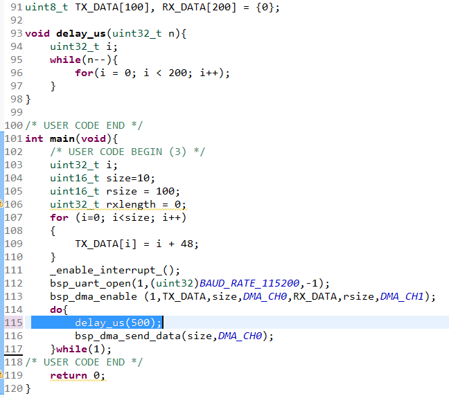
Delay Settings are shown in the figure:
I grabbed the waveform with an oscilloscope.
This is the normal output waveform without delay when debugging LIN port SCI mode of pin 131/132. The data sent is (0x55, 0xAA) and received normally (0x55, 0xAA).


This is the starting state waveform for setting delay and then sending data (0x55, 0xAA), which is a segment of random code.


This is the waveform after setting delay and then sending data (0x55, 0xAA) for a period of time. In the idle state of delay, as shown in the figure, there is always low level, similar to sending FF signal all the time.


