This thread has been locked.

If you have a related question, please click the "Ask a related question" button in the top right corner. The newly created question will be automatically linked to this question.

TM4C123BH6PM: Slave mode SSITx Timing spec on MODE3(SPH=1,SPO=1)

Part Number: TM4C123BH6PM

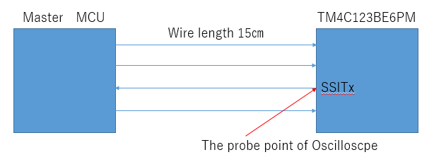
Hello, we are debugging TM4C123BE6 SSI Slave program.

We choose SSI Slave Mode3(SPO=1,SPH=1). But SSITx waveform is different from the Datasheet's description (Figure23-22).

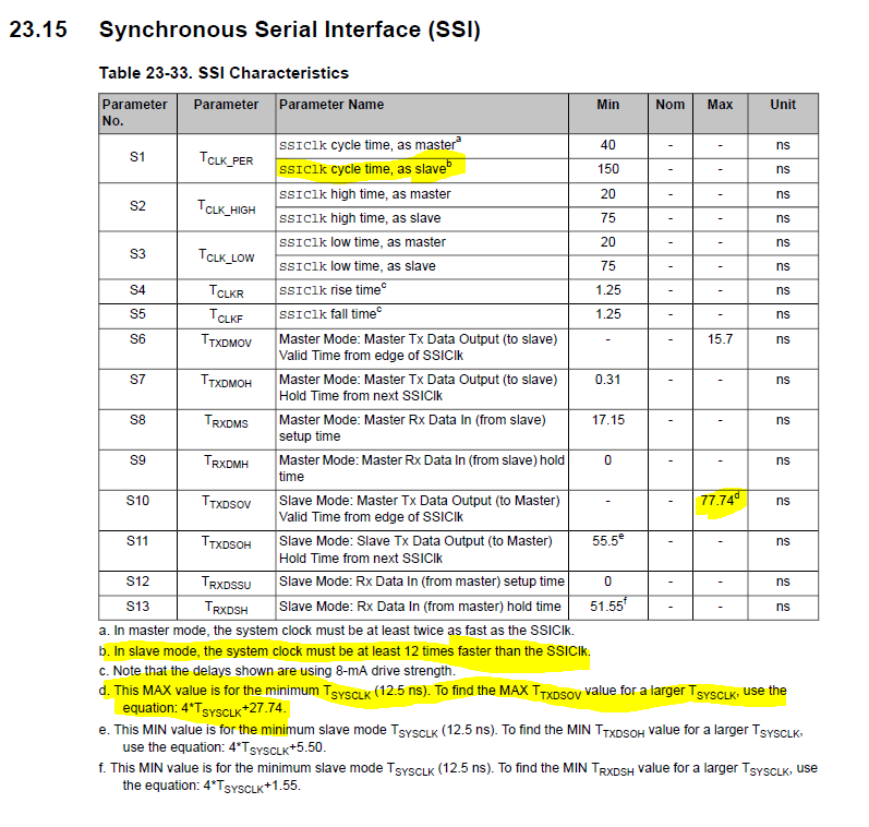
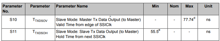
S10 and S11 Values are as follows;

We use the following SSIConfigSetExpClk function.

SSIConfigSetExpClk(SSI0_BASE, SysCtlClockGet(), SSI_FRF_MOTO_MODE_3, SSI_MODE_SLAVE, 6666666, 8);


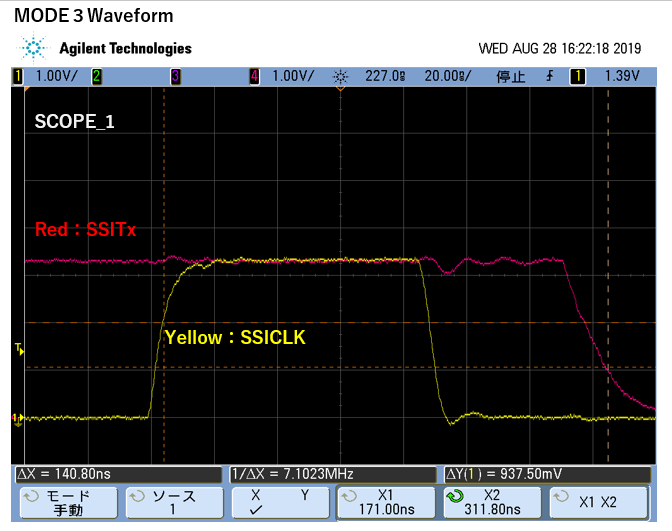
We want to use SSITx to meet MODE3 (Figure23-22) spec.

If there are any extra S/W settings in order to meet MODE3 spec ,please let me know.

Best regards,

ay0689_3

  • Greetings,

    While (others) here may be able to complete a (proper) diagnosis - my belief is that your scope cap would be (greatly) improved if it revealed at least '3 full SPI clock periods.'     In addition - the scope cap as posted reveals (only) an apparent, 'Constant Slave SPI_TX' level.     

    Would it not prove better to have the Slave transmit (either) '0x55 or its complement 0xAA?'    Either of those data bytes 'toggle the SPI data line' at the 'SPI clock rate' - enabling those here to (properly) view the key 'signal to signal' edges & transitions.    (which as now presented - are unseen!)

  • What speed is your system clock configured to? If not 80MHz, then you must adjust the maximum SSI clock rate and the S10 timing delay as described below.

  • Hello, Bob-san,

    Our System Clock and SSIClk settings are as follows, 

        System Clock FREQ.: 80MHz (12.5ns)

                  SSIClk FREQ. : 6MHz(166.666ns)

    It meets the datasheet TCLK_PER spec(S1). But  S10 value on the waveform is bigger than the spec value(77.74ns).

    Best regards,

    ay0689

  • In SSI_FRF_MOTO_MODE_3, the clock polarity is 1 which means data changes on the falling edge and is clocked on the rising edge. The delay time from the falling edge of the clock to the change in the slave's SSITX line looks to be about 40nS in your picture. (I measured 38nS in my setup.) This is less than the maximum specification  of 77.7nS.

    The issue is the waveform picture is not correct. The timing table is correct, and the picture in section 15.3.4.6 provides a better image of the relationship between clock and data for mode 3.

  • Hello Bob-san,

    thank you for your detailed explanation.

    I persisted on Figure23-22 diagram. So, I missed S10's intention.

    I add your comments and my understandings in the waveform capture.

    Thanks and best regards,

    ay0689

  • May it be noted that your latest 'Screen Presentation' proves 'inspired!'     Bravo - so vital a 'guide' MUST be quickly/easily found (stored for reference) - that's too often 'over-looked.'

    And - Swear to God - your opening post revealed 'SSI(Tx)' as 'flat-lined' - which prevented such 'signal to signal EDGE analysis'...    I noted that in an earlier posting, here.    (Screen-Cap was subsequently altered (edge added) - is that not true?)

    Firm/I have noted - that 'at times' (and depending upon the particular MCU's: Lot, Age, Temperature & Voltage) such 'Signal Edge Timing' will (progressively vary) with the length of the bit-stream.   (i.e. may 'improve' or 'worsen' - thus our suggestion of a 'Limited yet Multi-Bit Capture.'      Note: nothing herein is 'specific nor aimed towards this vendor'  - we likely noted this 'progressive timing variability' upon another's (possibly several others') MCUs.    

    It should be noted that this 'progressive, bit-edge timing variation' occurred at an industry giant - halted production - and our consulting team (w/great effort & good fortune) proved uniquely able to 'find & resolve.'    

    The 'Examination of ONLY a 'SINGLE BIT's EDGE TIMING' (as presented here)  - opens one to 'Missing' such 'Progressive/Additive Spec Violations!'    (thus justifying (this) and the (earlier) 'bypassed'  writing!)

  • ay0689,

    Your understanding is correct.