This thread has been locked.

If you have a related question, please click the "Ask a related question" button in the top right corner. The newly created question will be automatically linked to this question.

TM4C1290NCPDT: USB and CAN multiplexing

Part Number: TM4C1290NCPDT

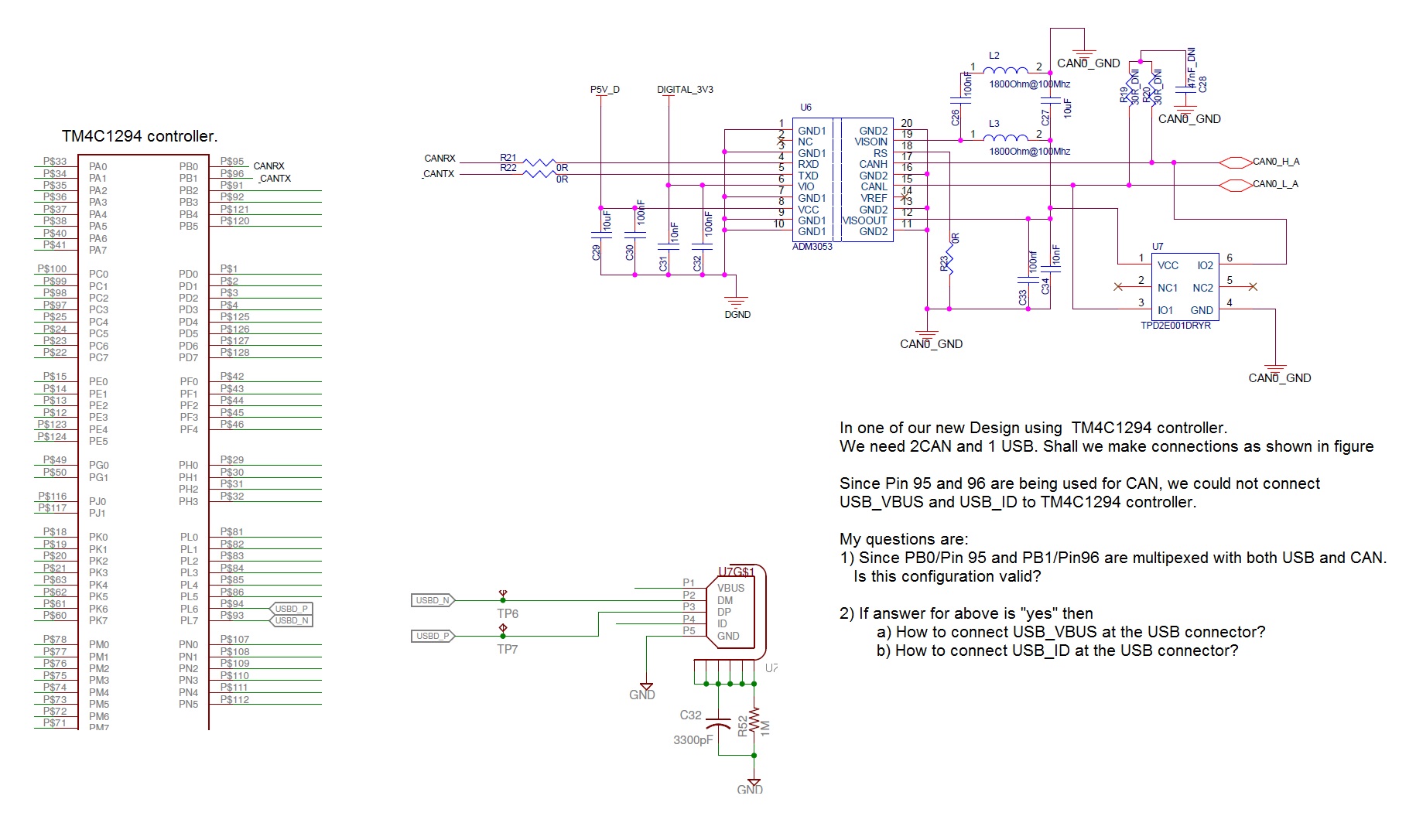
In one of our new designs using  TM4C1294 controller.

We need 2CAN and 1 USB. Shall we make connections as shown in figure (attached)

Since Pin 95 and 96 are being used for CAN, we could not connect USB_VBUS and USB_ID to TM4C1294 controller.

 My questions are:

1) Since PB0/Pin 95 and PB1/Pin96 are multipexed with both USB and CAN. Is this configuration valid?

2) If answer for above is "yes" then

         a) How to connect USB_VBUS at the USB connector?

        b) How to connect USB_ID at the USB connector?


Thanks in Advance

HARANATH V

  • Hi,

      Do you plan to use the OTG mode? My understanding is that the ID signal is only used in OTG mode. If you do not plan to use OTG mode then the PB0(95) can be used for CAN. VBUS is normally needed for OTG as well. However, if you need to monitor VBUS while in USB device mode then you can route the VBUS signal through a voltage divider to any of the GPIO pins for monitor. Please refer to the TM4C129 system design guideline for details. http://www.ti.com/lit/an/spma056/spma056.pdf Below is the excerpt from the application note. 

    4.3.1 USB Device Only
    For TM4C129x devices that are used in a device-only configuration, the only signal used in addition to
    USB0DM and USB0DP is USB0VBUS, which is located on port PB1. PB1 is 5-V tolerant. In USB device only
    mode, USB0VBUS is used to detect when voltage has been applied to or removed from the USB
    connector, which triggers software to manage the internal USB PHY accordingly.
    For a USB device-only configuration, a 100Ù resistor should be placed in series between VBUS on the
    USB connector and PB1 (or alternate GPIO) on the microcontroller in order to limit damage caused by any
    ESD events.

    If PB1 must be used for a function other than USB0VBUS, any other available GPIO could be used in its
    place. Because no other GPIO pins are 5V tolerant, a 5.6KÙ +/- 5% in series with a 10KÙ +/- 5% resistor
    should be wired as a voltage divider between VBUS on the connector and ground. This circuit drops the
    5V VBUS value to 3.2V at the GPIO pin.

    4.3.3 USB OTG
    TM4C129x devices that support USB OTG mode include the signals for USB Device mode, signals for
    USB Host mode and an additional signal USB0ID located on pin PB0. This USB ID signal is the 5th pin
    found on a USB micro-AB connector. If a micro-A cable end is plugged into this connector, the ID pin on
    the cable is tied to ground causing the TM4C129x device to operate as a USB host. If a micro-B cable end
    is plugged into the USB connector, the ID pin is left floating. In this case, the TM4C129x device's internal
    pull-up on the USB0ID signal causes the controller to operate in device mode.
    In order to limit damage from ESD events, a 100Ù resistor should be placed in series between the ID pin
    on the USB connector and USB0ID(PB0) on the microcontroller.
    To support full USB OTG negotiation using the SRP and HNP protocols, VBUS from the USB connector
    must be directly connected to USB0VBUS(PB1) of the microcontroller without a series resistor in between.
    In this case, USB0VBUS should be connected to an ESD suppressor such as a TVS diode, or ESD
    resistant VBUS switch.