This thread has been locked.

If you have a related question, please click the "Ask a related question" button in the top right corner. The newly created question will be automatically linked to this question.

CCS/TM4C123GH6PM: PWM pins in TM4C to drive motor

Part Number: TM4C123GH6PM

Tool/software: Code Composer Studio

Hi,

I am new to TM4C123GH6PM. 

The pin out lists multiple functionality of TM4C board. Which 6 pwm pins I can configure as digital , to generate digital outputs.

PD0 and PB6  are connected together as AnalogIn , what does it means and can I use both pins to generate digital signals and how?

Please explain in brief about how to use different functionality of pins and what to avoid/

Thanks,

Ayushi

  • Hi Ayushi,

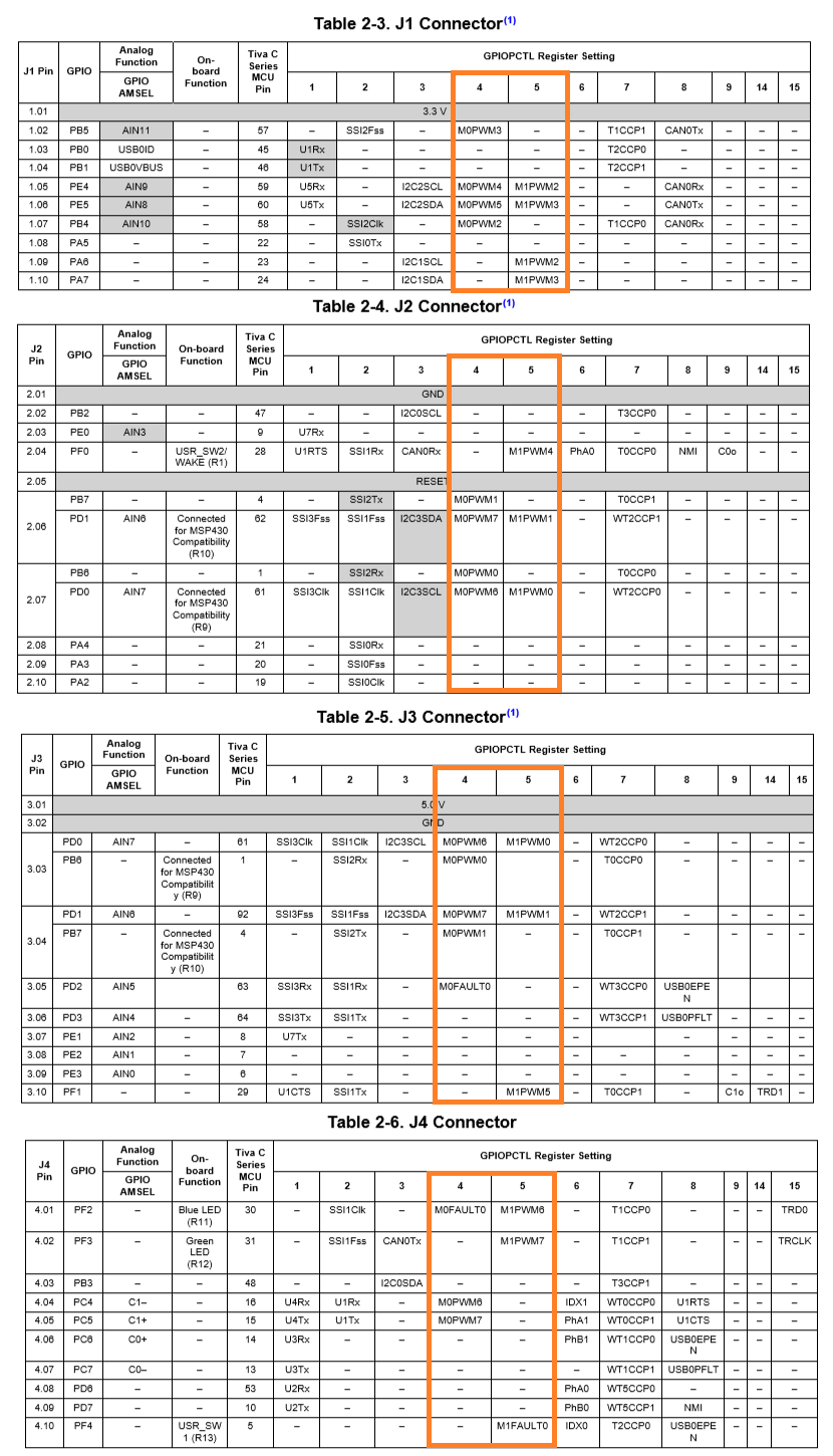
      As you can see in the below table from the datasheet, the PB6 is only a pure digital pin multiplexed with different functionalities. The PB6 can be configured as a SPI RX pin, a PWM pin or Timer Capture pin. The PD0 is another pin that is multiplexed with different functionalities. The PD0 can also be a ADC pin. If you want to use PB6 and PD0 as PWM pins you can certainly do so. For example, you can configure PB6 as a M0PWM0 pin and PD0 as either a M0PWM6 or M1PWM0 pins. 

      I will suggest you start with the PWM examples under <TivaWare_Installation>/examples/peripherals/pwm folder. You can start with the invert.c example. In this example, it configures the PB6 as a M0PWM0 pin. Below is a snippet of the code. You can go to the folder and view the entire source code. 

       //
        // The PWM peripheral must be enabled for use.
        //
        SysCtlPeripheralEnable(SYSCTL_PERIPH_PWM0);
    
        //
        // For this example PWM0 is used with PortB Pin6.  The actual port and
        // pins used may be different on your part, consult the data sheet for
        // more information.
        // GPIO port B needs to be enabled so these pins can be used.
        // TODO: change this to whichever GPIO port you are using.
        //
        SysCtlPeripheralEnable(SYSCTL_PERIPH_GPIOB);
    
        //
        // Configure the GPIO pin muxing to select PWM00 functions for these pins.
        // This step selects which alternate function is available for these pins.
        // This is necessary if your part supports GPIO pin function muxing.
        // Consult the data sheet to see which functions are allocated per pin.
        // TODO: change this to select the port/pin you are using.
        //
        GPIOPinConfigure(GPIO_PB6_M0PWM0);
    
        //
        // Configure the PWM function for this pin.
        // Consult the data sheet to see which functions are allocated per pin.
        // TODO: change this to select the port/pin you are using.
        //
        GPIOPinTypePWM(GPIO_PORTB_BASE, GPIO_PIN_6);
    
        //
        // Configure the PWM0 to count up/down without synchronization.
        //
        PWMGenConfigure(PWM0_BASE, PWM_GEN_0, PWM_GEN_MODE_UP_DOWN |
                        PWM_GEN_MODE_NO_SYNC);

  • Vendor Charles' response is proper - yet poster's quest included, 'multiple/additional requests.'

    Ayushi Thakkar said:
    Which 6 pwm pins can I configure as digital , to generate digital outputs.

    It appears likely that  poster's  board is the 'Basic '123 LPad.'    That particular LPad 'features' (PD0 dead-shorted to PB6)  as identified by our poster.    That 'feature' must be voided!    (which is achieved via the removal of (famed) 'Plague-istors' - R9 & R10!)

    Unknown is 'How/Why' this poster 'keys' upon '6 pwm pins' - there are more than double that number.    The '123 LPad'  User Guide details as follows: (below)    (Note that the chart provided by Charles was sourced from the MCU manual - it is expected that the  'LPad's Chart' would better reflect 'limitations' - likely imposed by the design of the small LPad's pcb...)

    Any of those PWM pins w/in Register Bank 4 or 5 are candidates for PWM Operation.

    Ayushi Thakkar said:
    PD0 and PB6  are connected together as Analog In , what does it means and can I use both pins to generate digital signals and how?

    As vendor's Charles mentioned - PD0 (as it appears w/in Register Bank 4 or 5) can function as an Analog Input.   PB6 (again as Charles noted) may generate your digital output.   As that 'LPad' has also 'dead-shorted' PD1 to PB7 - that 'pointless feature' must also be 'Corrected!'   (i.e. removed!)   Banishment of both R9 & R10 will restore the LPad to 'Normal & Proper' board operation...

    Ayushi Thakkar said:
    Please explain in brief about how to use different functionality of pins and what to avoid/

    Again - as Charles has noted - the API details 'How' one is able to 'Configure a Multi-Function MCU pin' - into your desired operating mode.   Your review of the 'Peripheral Driver Library Guide' proves especially beneficial.   (it is highly detailed)

    As to avoidance - use of 'DRM or (even worse) ASM' will needlessly prolong & frustrate your design effort.   Do not fail to study and understand the chart I've imported here for you.   Your desired 'Pin Mode' results from your proper Configuring & Typing of such 'Multi-functional' MCU pins...

    Your Subject Line reveals your intention to 'Drive a Motor!'    It is almost certain that this MCU (any MCU) is incapable of directly driving (most all) Motors!    It is normal/customary to employ a 'Power Driver' - which is inserted between the MCU & Motor - to 'Meet the Current Demands of most all Motors.'   Attempts to directly connect your MCU to (most any) Motor - is (almost) guaranteed to KILL your MCU!

    You may search for 'H-Bridge' - which proves a reasonably standard means of driving a Brushed Motor - under MCU Command & Control...

    Tag: How (really) to determine the (potential) role of each MCU pin 'exposed' via the '123 LPad.'

  • Hi cb1,

       Thank yo so much for providing this excellent information to the poster. 

  • Hi Charles,

    Thank you - poster MUST employ some Power Buffering between his MCU and the Motor!