Hello,
I'm currently working on establishing communication with an external ADC - the LTC1298. According to its datasheet, it uses SPI communication to initiate conversions and transfer its readings. Communication with the LTC1298 is half-duplex. As it is my first time working with the SSI modules in TivaWare, and SSI in general, I have a couple questions:
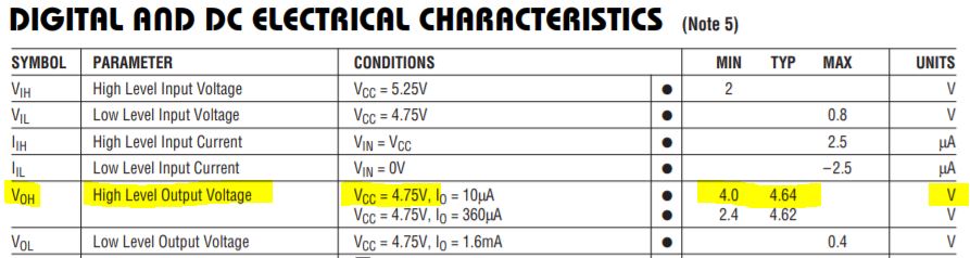
- According to the LTC1298 datasheet:
"The CLK synchronizes the data transfer with each bit being
From my understanding (and according to section 15.3.4.6 of the microcontroller datasheet), this corresponds to the following frame format: SSI_FRF_MOTO_MODE_3 (Polarity = 1, Phase = 1)?
transmitted on the falling CLK edge and captured on the
rising CLK edge in both transmitting and receiving systems."
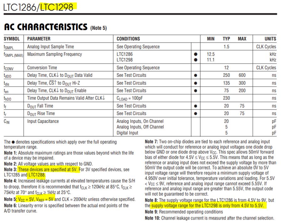
- The sampling rate of the ADC is 11.1 ksps, and the maximum SPI clock rate it 200kHz. What clock rate would you recommend in this case? Would 150kHz sufficiently account for the sampling frequency?
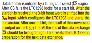
- "The data transfer is initiated by a falling chip select signal" - I understand that this part is handled by the TivaWare library upon calling SSIDataPut()? And that chip select returns to its original state after the message is sent?
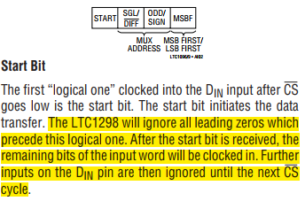
- According to the datasheet, the LTC1298 requires the following input data to start the conversion:
"After CS falls the LTC1298 looks for a start bit. After the
start bit is received, the 3-bit input word is shifted into the
DIN input which configures the LTC1298 and starts the
conversion. After one null bit, the result of the conversion
is output on the DOUT line."

- The conversion is output after one null bit, does that mean I should wait for at least 1 clock cycle before attempting to read the data in the receive FIFO, or does SSIBusy() handle this? Perhaps I should use SSI interrupts instead?
- I understand that I need to send this message manually to initiate the transaction, using SSIDataPut(). Will my message be sent MSB first, or do I need to reverse it? The last field in the message (MSBF) determines how the data is returned to the Master (MSB first or LSB first) - which option should I choose in this case - i'm assuming MSBF.
- Finally, the resolution of the ADC is 12-bits. I therefore set the data width parameter in SSIConfigSetExpClk() to 12. Will this work ok for both sending the initial 4-bit message, and then receiving the data?
Taking all this into account, would the following code work (I don't have a way to test it at the moment, and I need to continue with the remainder of the application):
//SPI configuration for LTC1298
SysCtlPeripheralEnable(SYSCTL_PERIPH_SSI1);
GPIOPinConfigure(GPIO_PD0_SSI1CLK);
GPIOPinConfigure(GPIO_PD1_SSI1FSS);
GPIOPinConfigure(GPIO_PD2_SSI1RX);
GPIOPinConfigure(GPIO_PD3_SSI1TX);
GPIOPinTypeSSI(GPIO_PORTD_BASE, GPIO_PIN_0 | GPIO_PIN_1 | GPIO_PIN_2 | GPIO_PIN_3);
SSIConfigSetExpClk(SSI1_BASE, SysCtlClockGet(), SSI_FRF_MOTO_MODE_3, SSI_MODE_MASTER, 150000, 12);
SSIEnable(SSI1_BASE);

while(1)
{
    SSIDataPut(SSI1_BASE, 0x0000000D);
    while(SSIBusy(SSI1_BASE))
    {}

    SSIDataGet(SSI1_BASE, &pui32Data); //pui32Data defined somewhere else
}
Thank you in advance for your help.
Regards,
Ksawery