This thread has been locked.

If you have a related question, please click the "Ask a related question" button in the top right corner. The newly created question will be automatically linked to this question.

EK-TM4C123GXL: ADC + DMA timing

Part Number: EK-TM4C123GXL

Hi there!

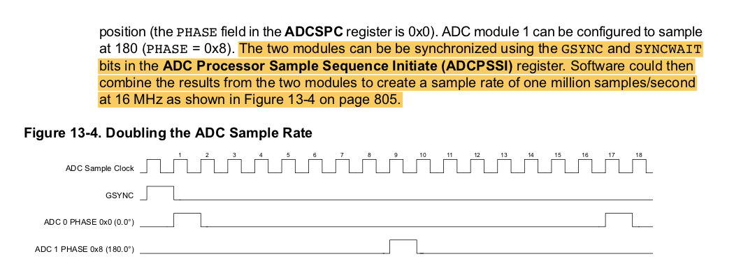
I am trying to sample an analog signal using the EK-TM4C123GXL evaluation board. I would like to control the sampling frequency of a single ADC up to the maximum declared speed of 1Msps. From my understanding the ADC would take 16 cycles @ 16Mhz from trigger to making the data available in the FIFO.

I would use the following setup:

- Use a General Purpose Time to trigger the ADC at the right speed (I guess that for a single sample the timer should count 80 clock cycles - if the CPU is running @80Mhz in order to trigger the ADC @1Msps)

- Use uDMA to transfer 1024 samples to a buffer in memory

- In the last uDMA interrupt stop the timer to end the AD conversion

While this is the general outline I came with a couple of questions I could not answer:

1. One idea was to setup the ADC SS0 to sample 8 measurements and trigger a ping-pong transfer on the uDMA side. 

- In this case each sample would be triggered independently by the timer or the whole train of 8 samples would be ran one after the other @16Mhz? In other words, am I able to control the speed at which the 8 measurements are sampled?

- I was thinking to trigger the uDMA every 4 samples. In this case the arbitration size would need to be 4. However, which should be the transfer size for the DMA buffers? Should it be 4 updated at every transfer, the total number of samples (1024) or each buffer would have to be setup with half of that?

2. Another approach could be to trigger via the timer a single measurement and transfer it to the buffer via DMA. Would this be feasible at 1Msps?

3. From what I understand the DMA would mask the ADC interrupts and emit only one completion interrupt at the end of the conversion or in case of ping-pong transfer mode after each transfer. Is this understanding correct?

4. Is there a simple way (using debugger, saving data into a variable, ...) to measure the real sampling frequency, meaning clock cycles from trigger to completion and make sure that the FIFO buffer is never overflown, considering that the interrupt from ADC would be masked by the DMA?

I am sorry if some of these questions are elementary/naïve. I am still learning microcontroller programming, so if you have any previous post, some code example or section of the datasheet I should read in more depth, please let me know!

Thank you for your support


  • Hi,

      You are not asking elementary/naive questions at all. You are really asking very technical performance/throughput questions that I really need to think before answering. :-)

    Daniele Barreca said:

    1. One idea was to setup the ADC SS0 to sample 8 measurements and trigger a ping-pong transfer on the uDMA side. 

    - In this case each sample would be triggered independently by the timer or the whole train of 8 samples would be ran one after the other @16Mhz? In other words, am I able to control the speed at which the 8 measurements are sampled?

    - I was thinking to trigger the uDMA every 4 samples. In this case the arbitration size would need to be 4. However, which should be the transfer size for the DMA buffers? Should it be 4 updated at every transfer, the total number of samples (1024) or each buffer would have to be setup with half of that?

    If you are going to sample 8 channels then I would suggest to transfer them out as soon as all 8 channels are complete. 

    Daniele Barreca said:

    2. Another approach could be to trigger via the timer a single measurement and transfer it to the buffer via DMA. Would this be feasible at 1Msps?

    Triggering on every measurement means the CPU will be interrupted more frequently. There may be other higher priority interrupts that may preempt or delay the servicing of the DMA interrupt. If CPU is to be interrupted on every measurement, then the CPU may as well just read the ADC measurement without using using the DMA.

    Daniele Barreca said:
    3. From what I understand the DMA would mask the ADC interrupts and emit only one completion interrupt at the end of the conversion or in case of ping-pong transfer mode after each transfer. Is this understanding correct?

    Yes,

    Daniele Barreca said:

    4. Is there a simple way (using debugger, saving data into a variable, ...) to measure the real sampling frequency, meaning clock cycles from trigger to completion and make sure that the FIFO buffer is never overflown, considering that the interrupt from ADC would be masked by the DMA?

    I think what you can try is to set a GPIO pin before triggering. Once the processor is serving the uDMA interrupt upon completion of the transfer you will clear the GPIO pin in the ISR. In the scope you can see the amount of time it takes to complete the conversion and the uDMA transfer. Something along this line is the idea, 

  • Charles Tsai said:
    You are not asking elementary/naive questions at all. You are really asking very technical performance/throughput questions that I really need to think before answering. :-)

    Great response from vendor's Charles - and duly, 'Seconded by our (outsider) design team!'

    Now you have 'specifically requested (we believe) the time between, "Trigger & Data Available w/in ADC's FIFO."     That's correct - is it not?    

    You have stated, "I would like to control the sampling frequency of a single ADC."    May we ask - is not the 'sampling frequency' (exclusive) of the 'added - pass-thru time - demanded by the FIFO?     And - is not 'usually' - the 'sampling frequency' of higher interest/concern/management - than the (longer) 'pass-thru time' - until the FIFO is loaded?

    We note that you, 'Cannot operate upon those ADC measures until the data 'becomes available' w/in the FIFO - under the scenario you've described.    That said - not always - is such ADC Data required with 'such immediacy.'   By contrast - the ability to, 'Properly capture analog signals at the 'highest possible rate' - is often sought.   

    Have you a real preference - and if so - why?    And if the 'highest speed analog signal 'capture' is the objective - how do you propose 'measuring that?'    (measurement IS required - so that you may (realistically & efficiently) 'optimize.')

  • Dear Charles,

    thank you very much for your input! I think I had misunderstood the right use of the sampler.

    I was thinking to use the sampler to sample from the same channel in order to trigger a "train" of measurements and then use the DMA to transfer them all to the buffer. However in this way I would not be able to control the sampling speed and from your answer I infer that the sampler is aimed at sampling from different channels (or from the same channel in case multiple measurements are needed for the same time-point, e.g. to average them).

    I now use a single-sample sequence and trigger the DMA to make 1024 transfers with arbitration size of 1 (this should mean that the ADC is triggered by a timer at the desired frequency, the sequencer converts one measure, the DMA is triggered after every sample and the interrupt routine is called when all of the transfers are completed). However, when I stop the debugger in the ISR, the overflow status of the ADC FIFO it is overflown unless the timer counts more than 165 cycles. Since the CPU is running @80Mhz, 165 cycles means 32+1 16Mhz cycles. This would seem to imply that the ADC is actually generating 500Ksps (and then uses one more cycle to trigger the DMA transfer, maybe?) and I hit a limit if I try to push it faster than this.

    To achieve 1Msps I had to activate the second ADC phase-shifted of 180° and in this case I can double the rate. This seems in line with what stated in the DS. However, from the picture in the same page it would seem like a single conversion would take 16 cycles, so in theory the two ADC working together could sample every 8 cycles, meaning 2Msps. I find this section (13.3.2.5) of the datasheet a bit counter-intuitive, can you help me clarify it?

    I have also a second question regarding the DMA, which might be simpler :) ... In order to save space I want to save the results of the conversion in a uint16 array. This means that I am setting up the DMA to read 16 bit from the ADC peripheral with a destination increment size of 32 bit (I am using two ADC shifted, so I would like to write the results at every second position in the array). If in the ROM_uDMAChannelTransferSet I give the first element of the buffer as destination address, I get that the 1st element is zero, the 2nd is full, the 3d is zero and so on, while I would expect the 1st el. to be full, the 2nd zero , etc... The hack that worked for me was to pass as destination address  (&g_ui16DstBuf[0]-1), but it looks rather ugly and might try to access the wrong memory address. Is there any way I can achieve the same result with a clean construct?

    PS: since I don't have access to a scope I tried to measure a PWM signal at 60,606 KHz (165*8 CPU cycles) with 50% duty cycle. If the ADC runs at around 1Msps (1 sample every 80 cycles) this should give me 8 samples in the HIGH state and samples in the LOW state for every cycle, and this works confirming somehow that the combined ADCs are running at the desired speed.

    Thank you again for your support!

    Regards,

     Daniele

  • Dear cb1,

    You are right to note that I don't need the data immediately for processing and what I really need is to store the data in memory as fast as possible and then process it later on. You are also right to make me notice that I should care only about the sampling frequency, not about the pass-thru time. However, it is important for me to know the sampling+pass-thru +DMA read time in such a way to trigger the ADC at a speed selected in a way that doesn't overflow the FIFO (and then lose the data)...in other words when the ADC finished the conversion it should find the FIFO empty.

    Regarding the measurement I proposed a strategy in my answer to Charles, which measures a square wave with a known frequency and then counts how many samples are taken during each semi-period to have an idea of the sampling speed.

    Thank you for taking your time and regards,

    Daniele

  • Hello Daniele,

    Thank you - interesting comments from you (and you do NOT have to agree w/staff's or my view.)     You  may  note that my team is (~75%) young women - and that (a growing number) of our clients are, 'Women Owned/Managed' Tech Firms!    Staff (and I) are 'so glad' to welcome you here...

    Let's break-down your (neat) writing:

    DB: "What I really need is to store the data in memory as fast as possible and then process it later on."   

    • That's (almost) correct - perhaps (even) better would be, 'To Acquire the input Analog Signals as fast as possible'
    • and then - (properly) post acquisition - safely store that data so it is not 'lost.'
    • finally arrives 'processing' - usually revolves around, 'What you'll do w/that data.'

    DB: "Make me notice that I should care only about the sampling frequency, not about the pass-thru time."

    • Again - almost.    Should not you care about, 'All of the above' - and (somehow) attempt to identify those items - most impactful?
    • should not that attempt, 'Target the discovery of the 'time demanded and/or expended - w/in each of your, processing operations?'
    • and 'might the order' in which you manage that processing - produce 'differing results?'    Might that be a 'good thing?'    Why?

    DB: "... proposed a strategy in my answer ... measures a square wave (known freq.) and then counts how many samples are taken."

    • Might an alternative method to, 'Best Determine the (actual) sampling frequency' (and its 'consistency') result from your, 'generating an accurate, linear-ramping voltage signal - applied to 'one' of your ADC Inputs - w/the ADC Sequence set for '8 sequential (back-to-back) conversions?'   (Sequence '0' iirc)    *** Your 'square-wave' method is a 'bit brutal' as the 'voltage swing' from (near) VDD to (near) Gnd cannot be 'immediately' registered by the ADC - due to the ADC's 'Capacitive charge/discharge effects.'   (thus justifying - our more 'gentle' approach!)
    • The voltage 'delta' - between each successive ADC reading - provides (my group believes) the 'truest indication' of the (actual/REAL - 'moment of analog capture') sample time you're achieving.
    • this proves true providing the linear ramp substantially spans the 'full, legal voltage range' of your ADC & the 'Sequence of 8 ADC readings' was selected. 
    • note that in the real-world - it proves 'unlikely' that you'd be, 'Able to maintain that 'Scanning Rate' as it is achieved (minus) any processing!    (which will be required prior to your 'next sampling sequence!)
    • it may - or may not - prove that, 'Your entire Acquisition & Processing' operation 'feeds back' to your 'Sampling Time.'    (i.e. you may 'Acquire too fast - or too slow' - how - or (even) can that be possible?    If so - what then?)

    And - to throw (yet another) 'monkey wrench into this witch's brew' - you seek to, 'Add the µDMA to the mix!'    Young staff here asks, 'Should that be attempted in 'One Gulp?'    (without attempting to develop answers/understanding - to items listed?)     (Staff advises -  'As the ADC's FIFO limits the amount of data available to the µDMA' - is that 'addition of complexity' properly justified - in your application?)