This thread has been locked.

If you have a related question, please click the "Ask a related question" button in the top right corner. The newly created question will be automatically linked to this question.

EK-TM4C1294XL: ADC resolution mid supply

Guru 54808 points
Part Number: EK-TM4C1294XL
Other Parts Discussed in Thread: TL081, LM741

Single ended analog input signal 1.65v threshold has poor digital granularity for magnitude changes > +/-100mV relative mid VREFP.

How can ADC single ended sensitivity be improved so even +/-50mV steps increase or decrease register values >100mV relative mid VREP?

All magnitude changes >100mV flat line near mid supply and scaling by 4096 is mostly NULL. Otherwise not from 0v up to 1.65v or even up to VREFP 3v3 on single ended inputs. 

Seemingly we need to make 1.65v produce 0x0 register integers where each 50mv = 0x3E8 or +/-1000 relative to ADC scale factor 4096. This seems impossible to achieve from any single ended input. Yet other TI forum claim an OPAMP output to any single ended ADC input channel produces correct digital translation from mid VREFP. That claim seems misleading as it can not be achieved with any granular results >100mV and makes OPAMP appear to have very bad precision. Why some TI people make it so complicated and obviously mislead others in the process is baffling or even intentional.

ADC single ended input seemingly has no way to process a bipolar signal from 1/2 VREFP with any kind of refined granularity, e.g. >100mV relative mid VREFP.  Please enlighten us all how it can be done with examples of working software or ADC configurations for single ended inputs. Seemingly double ended ADC inputs must be combined for the single ended OPAMP signal produce correct results from mid VREFP with >100mV granularity in either direction.   

  • Hi BP101,

    Gl said:
    Single ended analog input signal 1.65v threshold has poor digital granularity for magnitude changes > +/-100mV relative mid VREFP.

    When the ADC is used properly, that is not true. We have had this discussion before. If you are having trouble with ADC conversions on your custom board, please describe the circuit, the input signal and the sample routines you are using and I will try to help you. I do not have the time to create examples just to disprove your unsubstantiated claims. Don't get me wrong. I believe that you are not getting good results on your board with your software, I just don't believe your claim that it is a problem with the part.

  • Hi Bob,

    It's a launch pad not custom PCB revisited with more experiments. Well it seems differential mode produces to fine of a granularity. The individual steps produce a huge digital scale factor over single ended with the same bipolar signal. Meaning samples from a unidirectional current signal produce fine steps from VREFN - VREFP in very tight granularity.

    Yet a high frequency bipolar input signal in either input mode (single/differential) can not linearly track the magnitude of the signal. The differential samples remain locked VINcm (1.65v +/-100mV) no matter any formula configuration or charge share arrangement. Some how current flows out or into the channel keeping Cadc charged to 1.65v rather than the linear steps in the bipolar signal. Again that does not occur via unidirectional current signal as several experiments form a control scenario. 

    So the single ended channel can track a unidirectional current signal but not a fast 12-40kHz bipolar signal. When the magnitude of the slope increases the digital conversion is simply wrong, 2x Nyquist rate even worse. Yet unidirectional current signal when the voltage magnitude increases so does the linear slope correctly follow it.  Some kind of DC latching occurs with high frequency bipolar input signals that is not present with unidirectional current signals input in either channel mode. 

    How to stop Cadc from latching even with 4k7 RS 1nf of AINx channel load? Excessive current seems to flow from high frequency bipolar signal between these devices keeping Cadc charged or latched up. Is there some kind of ADC circuit trick to stop bipolar latching of Cadc? Has TI investigated open loop gain in certain amps may lead to this very mayhem being described? There was very same current flow latching present in competitions amp too. That seems to point finger at the ADC configuration or silicon design has underlying issues.

  • The TM4C ADC supports differential inputs, but not bipolar inputs (in which one or both inputs go below GND). See page 1066 of the datasheet.

  • Bob Crosby said:
    he TM4C ADC supports differential inputs, but not bipolar inputs (in which one or both inputs go below GND).

    The amps output is bipolar derived from 1.65v quiescent set mid supply (3v3) relative to VREFP 3v3, output never goes below ground in either mode but is considered a negative ADC value <1.65v >VREFN. The unidirectional amp mode, output moves from 0v up to <200mV of VREFP. That mode sort of works but clamps the negative portion of the input cycle up to (-4v) to ground (VREFN). So half the input information is being lost each cycle in unidirectional mode.

    For the differential test I tied the Odd AINx of pairs to ground and the Even AINx to the bipolar output, quiescent +1.65v. Neither ADC mode works for amps tested with reference set to 1.65v quiescent.  

  • Bob Crosby said:
    The TM4C ADC supports differential inputs, but not bipolar inputs

    Seemingly datasheet should use the word zero crossing. Bipolar can refer to voltage being divided it two unique polarities relative to a reference voltage or quiescent of the total, this case mid supply. Voltages >1.65v produce positive singed integer values and voltages <1.65v produce negative signed integers. That is so very bipolar.  

  • Hi Bob,

    Perhaps the ADC is working correctly in differential mode and the amps bipolar output is not scaling linear. Given a vertical ray, zero position (mid supply) never moves in the amps output as the integers increase or decrease in value. Perception being typical DMM digital readout has vertical slope when measuring the very same current points. One naturally questions why the differential amps output does not add vertical slope relative (mid supply) as both magnitudes increase in visual scope monitoring. Perhaps SW is required to make HW function as expected but that adds questionable complexity and invites precision errors.

    Seemingly a single differential amp is not capable alone to add linear slope relative to (mid supply) division of zero crossing inputs. Again typical DMM digital readout sets long standing precedence for how a device should function in the digital realm perspective of them, not to forget older analog meters too. The single differential amp mid supply behavior distorts reality of how measured events actually occur in these systems. The TM4C1294 ADC simply follows along forcing the same fictional zero crossing events on amps output which is never fully examined in TI datasheets or other text as being unrealistic to begin with.

    Seemingly it requires 2 differential amps where the first one manages 0-VREFP magnitude changes and second amp handles mid supply changes of vertical slope via first amps changes to the reference. TI sensors datasheets have not made that aspect at all clear or investigated said phenomena in said perspective. In today's world especially after Apollo moon flights some engineers expect all in one packages to do exactly that, e.g. less is more! 

  • Hi Bob,

    Hope you understand the Opamp monitors zero crossing events on it's input and output as bipolar events centered around mid VREFP or directly from 0v up to VREFP depending on the desired configuration. The mid VREFP centered and bipolar output events occur where the center (1.65v) remains fixed in that configuration.

    My point was the amp does not work properly in the centered mode as intended or desired. It can not produce a sloping digital representation of zero crossing  events from a fixed center output for the intended stated purpose of the device, with TM4C1294 ADC. I have never seen it properly work in several years of experiments with it and others like it from mid VREFP input state into ADC channels. It would be nice to know if the ADC has some kind of limitation stopping it from producing an accumulation slope in 240us intervals. Otherwise there is a lot of hype around a false narrative that mid center method is even prudent or truly a correct mirror of the actual physical events.

  • Gl said:
    It would be nice to know if the ADC has some kind of limitation stopping it from producing an accumulation slope in 240us intervals.

    There is no issue with the TM4C129 device ADC doing conversions every 240uS of an input voltage ramping past the reference midpoint provided the ramp speed is not faster than what the sample rate can handle.

    No, I do not understand what you are doing with the op-amp. If the issue is about how to use the op-amp, I will leave that discussion for others. If you still have an issue with the ADC, then perhaps providing a schematic of the op-amp circuit would help. Words are often inadequate when we have different definitions for terms.

  • Bob Crosby said:
    There is no issue with the TM4C129 device ADC doing conversions every 240uS of an input voltage ramping past the reference midpoint provided the ramp speed is not faster than what the sample rate can handle.

    I was referring to samples taken from fixed mid VREFP in single or differential mode can not accumulate or produce positive magnitude slope >100mV from 1.65v center. The more I experimented to try and make it work the more baffled at some belief inductive current even has such artifacts from ground side to begin with. Just because ADC can produce +/- samples from mid supply does not mean that is a correct method to measure bidirectional events that may have a linear moving center point artifact to being with. Forcing the amplifier output fixed to mid VREFP does not work as it should, relative to know DC theory of inductive events behavior. 

    That produces arbitrary data taken from ground side zero crossing events translated into fixed mid VREFP differential samples. The FIFO digital values do not relate to the actual inductive bidirectional events existing well above ground. That adds further to the confusion long standing precedence set by theory decades old.  Other TI forum did not produced Wiki that proves fixed mid VREFP (1.56v) is even prudent for the effect of accelerating inductive DC events. Yet they remain adamant argue fixed mid VREFP is proper even when Tina models show different results for the device and the real world results prove it is not at all correct to make such claim and no white paper to back it up.

    Seemingly it requires 2 amplifiers from ground side to reproduce the bidirectional artifacts from a sloping linear magnitude in either direction with in said slope relative to SAR step approximation granularity. There must be some reason why issue has been overlooked even in the latest TI experimental sensors. Perhaps certain test equipment misleads yet expects engineers to correctly interpret the visual results pertaining to DC theory, not just relying on scopes visual artifacts as being actual proof. Certain signals are difficult to view DC coupling while AC coupling widens visual, hence unnatural zero crossing events seem to occur. Yet the SAR can accumulate very little digital slope as artifacts swing equally in both directions from a fixed mid VREFP. Two amps could seemingly achieve 0-VREP bidirectional (min/max) variable sloping linear samples without output ever being fixed to mid VREP.

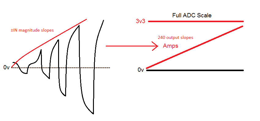
    Below diagram indicates required sample slope (right) achieved from a zero crossing ground side events (left). The single amp is incapable to create this required ADC signal for a correct successive approximation register of (bidirectional) events. Yet Tina Spice model plots produces same exact behavior below from a single amplifier and the real world device does not. The SAR forced to mid VREP produces samples shown on (left) have no true meaning relative to typical PI controller or other application variables. Hence a misleading narrative was born in several industry datasheets without clarification for its purpose relative to PWM modulation technique, should that even matter.  

  • Perhaps try experiment via cloud scope widget to plot a sloped line acquired from zero crossing bidirectional samples taken mid VREP. Compare the results side by side with digital values produced by DMM. Momentarily load down the sampled DMM measured source by some means. Does the scope Widget trace show as a narrow curved line moving upward with short hairs riding along it in either direction? Or do both sides exist along the very same vector, only growing in magnitude but without any vertical slope?   

    If your answer is the latter, how can that remotely represent via DSP what is truly occurring in real world events? The point being the negative half cycle is being lost in the non mid VREF configuration. So we are forced to monitor by means of VREFN-VREFP and loose half the required data. A similar high BW amp configuration seems to WA this very issue of missing vertical slope but it's a little late to step backwards in time. 

  • Bob Crosby said:
    Words are often inadequate when we have different definitions for terms.

    No kidding and the electronics industry has not clarified FO = 1/2 (VREFP - VRFEN) as a bipolar artifact. What else should the signal signature be called as the center point is fixed along the horizontal axis, zero crossing. Most early experimenters with OP amps came to know at one point in time singled ended supply amps could not produce a bipolar input on the output even above ground. Then late 70's along came the LM741 and TL081 recalling both were capable to re-produce a bipolar input on the output above ground, dc coupled. Others types required split dc supply, could only produced a zero crossing bipolar signal.

    Later modified the experiment so the amplifier could produce the needed signal for the ADC single ended input, 0-VREFP. Oddly the amps output still remained clamped on ground but both +/- zero crossing cycles were present in the output as the PI controller required. The point of experiment was to show how 1/2 the samples were being lost by the original configuration of amplifier. Neither configuration of amplifier per datasheet figures produces a fully qualified signal that represents replica or true RMS events for the ADC to converge upon.

    Below CH1 zero crossing input into amp, CH2 output produces zero crossing 1/2 cycles on the output. One would think scope evidence might spark some interest in that forum to investigate why the amp as configured from datasheet can not produce a replica signal the SAR can easily digest in single or differential mode from replica zero crossing events. Note the inverting input is not tied directly to ground in this capture, rather inverting input has 510k to ground. So the output produces zero crossing 1/2 cycles, phase shifted by 90° as LM741 graph shows 10Khz-100kHz input will shift the phase other type amps do too.

  • Perhaps TI engineers could invest in analog current meter (below link) to put in series with any load. Should inline events actually swing +/- directions equally with/to PEAK, said meter needle might swing wildly from DC events or vibrate 1/2 peak events? Most current clamps being inductive seemingly produce a false perspective of the actual DC inverter line events. At least the analog meter might produce some contrasting events to compare.

    Seemingly we are asking far to much of the SAR ADC to acquisition 20kHz bidirectional events when the attached HW is not producing a fully compatible signal replica of the original events. The sensor needs to produce both zero crossing events at the same acquisition level for the ADC to accumulate slope in those very same events as a analog meter should indicate as truth be told. Either I am wrong or exactly correct and no force in this universe can fix what was not meant to be without modifying the sensor circuit to work correctly for the intended purpose. Yet some TI forum would rather argue datasheet points versus finding real world solutions.

    www.facebook.com/photo.php


  • Below is a capture of the same amps single ended unidirectional output (0v-VREFP) derived zero crossing input events. Notice periods of missing cycles produce large voids in samples adding several milliseconds between 240us(4.17kHz) sample rate 2MSPS. Yet the ADC produces a fairly accurate slope of upward loading events. The downward sampled events are not as pristine, amplifier being forced to datasheet configured uni direction mode. 

    Contrast the above posted capture with below reveals uni sensor omits zero crossing input events omits explanation for such a sacrifice even being required. So the Other MCU forum becomes deluged with posts asking what up with the TM4C1294 ADC.

    TI forums need to cooperate find reasonable circuit solutions for knowledgeable customers who are not easily bamboozled by unsubstantiated datasheet sensor purpose and use claims. In this case the inverting input tied to ground does not allow differential amplifier output zero crossing events when reference pin is on the same ground plane and defeats one purpose for sensor claims. One purpose for the sensor explains replacement of typical high bandwidth discrete amplifier, addition of non precision components also known to produce bidirectional samples into the single ended ADC (above post capture). How could bidirectional typical application using high bandwidth amps be so easily dismissed? 

    CH1= zero crossing input, CH2 output to ADC missing positive half cycle. Wiki report (below) illustrates being inversion of the zero crossing input. Appears the Wiki report is correct and some forum gurus argue this very point after being alerted to the Wiki report still claim it does not relate to this sensor behavior. Scope capture argues indeed it does relate to Wiki report.