This thread has been locked.

If you have a related question, please click the "Ask a related question" button in the top right corner. The newly created question will be automatically linked to this question.

CCS/TM4C123FH6PM: Problems with clock configuration when using the chip without crystal

Part Number: TM4C123FH6PM
Other Parts Discussed in Thread: EK-TM4C123GXL

Tool/software: Code Composer Studio

Hello Everyone,

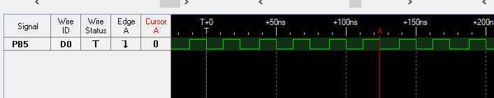
I am trying to use the chip with the internal oscillator and using the following configurations and switching a pin to observe the clock frequency but the frequency I am reading is quite low. 

Using the following configurations I get the waveforms: 

SysCtlClockSet(SYSCTL_SYSDIV_1 | SYSCTL_USE_OSC | SYSCTL_OSC_INT | SYSCTL_XTAL_16MHZ);

SysCtlClockSet(SYSCTL_SYSDIV_2_5 | SYSCTL_USE_PLL | SYSCTL_OSC_INT | SYSCTL_XTAL_16MHZ);

Any ideas on why I am getting such a low frequency? 

Thanks.

  • Hello again,

    Appears your "Crystal-Less MCU (main) oscillator issue" is behind you ... good that.

    It is not fully clear, "Exactly what you are seeking?"    Staff's best guess is "System Clock Frequency"   

    You've not identified:

    • to which MCU pin you've attached - and why (that) specific pin?
    • by which means you are causing that pin to toggle?

    Check - & confirm that (any) of the MCU's Timers are driven by the System clock.   If that proves true - might this method prove (more) insightful?

    • select one of the MCU's Timers & configure it for PWM (output) mode.    (50% duty cycle - that output will appear upon the Timer's pin)
    • scale the Timer's output frequency down (at minimum by  40x) ... this so that the 'MCU's Timer Output pin' can (actually) toggle at that rate   (i.e. 80MHz/40 = 2MHz - which the MCU's GPIO (may) be able to reach...

    Employing a code-block to toggle an output (as we assumed you've done) fails to achieve full GPIO output rate due to programming induced (slowing) influences.   (i.e. loop overheads, normal code execution cycles,  etc.)

    You may benefit by, "Adopting this 'check' as part of your normal Coding Practice."     We do so - and such output is automatically checked by our production equipment.   (i.e. just one of our (many) board-checks)    After a brief period that, "Timer in PWM Mode" code may be halted - and that pin, "Re-Purposed for other use..."

  • I am trying to set the clock to 16 mhz that is present on the internal oscillator.

    When I toggle a pin (In this case f3 but any pin shouldn't matter.) I want to see that I am able to toggle it at that frequency to prove that the clock is running with that frequency.

    Because the toggles are much slower that leads me to think the clock is running slower than it should run.

    Best,

    Tuna  

  • Nein, nein, nein!

    Re-read the earlier posting - toggling a gpio via code -  is NOT able to accurately "advise & inform" of the System Clock's actual frequency.

    Again - any Timer - set as (above) detailed/described - is a far superior (i.e. much more accurate) method.

    You should not expect (any) GPIO pin to toggle (much) beyond 2MHz (robustly) - that is NOT their design intent.     And proves true for all MCU vendors.

    Everything you 'seek' was listed in that initial post...     (Scaling the Timer's Output will enable the MCU's Output pin to 'keep pace.')

  • I am not sure what routine you used to toggle the pin. I wrote a routine that uses a timer pin that toggles at half the system clock frequency. I measured 8MHz using the first configuration (system frequency of 16MHz) and 40MHz with the second (system frequency of 80MHz). I also measured a system frequency of 16MHz using the external crystal on the EK-TM4C123GXL and the same system frequency with no call to SysCtlClockSet() as running from the PIOSC is the default. 

    //*****************************************************************************
    //
    // Configure Timer1B as a 16-bit PWM with a duty cycle of 50%.
    //
    //*****************************************************************************
    int
    main(void)
    {
    #if 0
        //  16MHz with external crystal
        SysCtlClockSet(SYSCTL_SYSDIV_1 | SYSCTL_USE_OSC | SYSCTL_OSC_MAIN |
                       SYSCTL_XTAL_16MHZ);
    #elif 1
        // 16MHz with PIOSC
        SysCtlClockSet(SYSCTL_SYSDIV_1 | SYSCTL_USE_OSC | SYSCTL_OSC_INT | SYSCTL_XTAL_16MHZ);
    #elif 0
        // 80MHz with PLL
        SysCtlClockSet(SYSCTL_SYSDIV_2_5 | SYSCTL_USE_PLL | SYSCTL_OSC_INT | SYSCTL_XTAL_16MHZ);
    #endif
        //
        // The Timer1 peripheral must be enabled for use.
        //
        SysCtlPeripheralEnable(SYSCTL_PERIPH_TIMER1);
    
        //
        // For this example T1CCP1 is used with port B pin 5.
        // The actual port and pins used may be different on your part, consult
        // the data sheet for more information.
        // GPIO port B needs to be enabled so these pins can be used.
        // TODO: change this to whichever GPIO port you are using.
        //
        SysCtlPeripheralEnable(SYSCTL_PERIPH_GPIOB);
    
        //
        // Configure the GPIO pin muxing for the Timer/CCP function.
        // This is only necessary if your part supports GPIO pin function muxing.
        // Study the data sheet to see which functions are allocated per pin.
        // TODO: change this to select the port/pin you are using
        //
        GPIOPinConfigure(GPIO_PB5_T1CCP1);
    
        //
        // Configure the ccp settings for CCP pin.  This function also gives
        // control of these pins to the SSI hardware.  Consult the data sheet to
        // see which functions are allocated per pin.
        // TODO: change this to select the port/pin you are using.
        //
        GPIOPinTypeTimer(GPIO_PORTB_BASE, GPIO_PIN_5);
    
        //
        // Configure Timer1B as a 16-bit periodic timer.
        //
        TimerConfigure(TIMER1_BASE, TIMER_CFG_SPLIT_PAIR | TIMER_CFG_B_PWM);
    
        //
        // Set the Timer1B load value to 1. From the load value (i.e. 50000) down to
        // match value (set below) the signal will be high.  From the match value
        // to 0 the timer will be low.
        //
        TimerLoadSet(TIMER1_BASE, TIMER_B, 1);
    
        //
        // Set the Timer1B match value.
        //
        TimerMatchSet(TIMER1_BASE, TIMER_B, 0);
    
        //
        // Enable Timer1B.
        //
        TimerEnable(TIMER1_BASE, TIMER_B);
    
        //
        // Loop forever while the Timer1B PWM runs.
        //
        while(1)
        {
        }
    }
    

  • Hello cb and Bob,

    Thanks for the answers. Coming from 8 bit processors I am really used to toggling any pin to measure the system frequency.

    I just used pin write function calls to do the toggling.

    I didn't realize there were limitations on toggling speed. (These probably come from using Tivaware HAL Library).

    I am able to observe the clock speed with the code you provided. 

    Tuna 

  • Hello Bob,

    While our answers substantially overlapped - staff & I doubt that the '123 MCU could drive its output pins to (either) 16MHz and (NEVER) to 40MHz!    Again - this is "MCU GPIO Reality" - no 'knock' upon your firm/devices!

    You chose the word 'measured' yet the logic analyzer displayed "Superb Square Edges" (perhaps somewhat 'wishful') - which (it is doubted) that a (proper) scope-cap would confirm!

    To remain w/in "reasonable" MCU-GPIO output specifications - when the System Clock was set to 80MHz - we configured the Timer to "Divide by 40" - so that (again) "reasonably square-waved 2MHz was output..."

  • CB1,

    You make an excellent point, and I would never create a real application driving a timer pin at 40MHz. However for this quick verification, it worked. Yes the logic analyzer squared up what must have been pretty ugly edges. Using a 500MHz sample rate on the logic analyzer and a 1.90V threshold, I received a good verification that the pin was indeed trying to toggle at 40MHz.

    Thank you for pointing out that to get good clean signals, using a divider to get to 2MHz or below is the best policy.

  • Bob,

    Thank you - appreciated.    Of course you realized those "necessary MCU limitations" (imposed by all MCU vendors) yet it is believed that (many) 'forum others' would benefit from such detail.    (clearly the poster 'learned')

    Staff notes that, "More & more applications" seek & benefit from such "HF clock signal injection" - yet beyond 2-3MHz most MCU outputs may prove inadequate.

    Should several HF clock signals (say 3 - 30MHz range) be required - "Multi-Frequency, Programmable, Output Clock sources" may prove optimal...    Crack staff is (already) working on the means to, "Frequency UP-CONVERT - employing the TM4C as a, "Programmable (sub 2MHz) Low Frequency Driver" which is then "Properly power boosted & Frequency-Scaled Upward!"

    Pity that "Resolving Green" only flowed once - staff's response was timely, nicely instructive (solely noted MCU output limitations!) & Spot-On!   (they deserved better...)

  • Hello Bob and CB,

    I am not toggling a pin faster than 2 MHz on my design but where would I get such insight without encountering the problem I faced if I were to go directly from the data sheet.

    Is it just coming from experience that you get by working on designs or is it something obvious I miss from the documentation?


    How would I evaluate the innate limitations on the architecture or the HAL libraries especially if it is not explicitly stated on their documentation? 

    Thanks.

    Tuna 

  • Hello,

    Not all of one's desires can be anticipated - and satisfied - even w/in a (near) 1500 page MCU Manual.     Such proves true w/in: Law, Medicine & all of the physical sciences.

    It was sensed that you had (hoped) to view an (again, near) 16MHz signal from a GPIO pin.    While the System Clock may reach such speeds - it is rare that (any) input or output (I/O) port - equals such capability.    This proves true as most all modern "MCUs, FPGAs & (similar)" most always operate "Synchronously" - and must "Qualify and Align" their I/O signals with one or more clocks & gated logic.   These requirements often operate in cascade - thus (further) reducing the fully specified frequency of (both) inputs & outputs.

    One can learn much via focused experimentation - attempt to drive an output at different rates - while applying a 'standard' load & monitoring the output signal for declining quality.

    Staff's search of the '123 MCU Manual found no, "clear, definitive spec" yet found:

    The parameters T_GPIOR & T_GPIOF provide (some) indication of the MCU's output capability - (i.e. the roughly 22nS combined value (realized @ 8mA) translates to ~45MHz ... yet no provision has been made for the various "Synchronizations" which the MCU enforces upon most all signals - and further limits 'I/O' frequency...

    Your gracious 'award' is appreciated by this young, uber smart & highly motivated Tech Staff!

  • You can get an indication of the limitations of the I/O pins from the rise and fall times in the datasheet (page 1347). Keep in mind that these times are with no load on the pins. As seen from the table, using the standard 2mA buffers it takes 16.1nS rise time and 29.4nS fall time. To achieve 20% to 80% square wave, you can go no faster than 1/(2 x 29.4nS) or 17MHz. That freqeuncy degrades quickly when you add any load to the signal. 

    The TivaWare library was designed to make interfacing to the hardware easier. Often execution efficiency is sacrificed for ease of use. I can make the I/Os toggle faster by writing in assembly language with direct register writes, but the time it takes to write such code is exponentially longer. (Also, it takes much longer to debug.)

  • Hello again, Bob,

    Once more - there is "high overlap" between our responses.    (ours - due to "Strength of Numbers" - about 20 minutes earlier)

    Gurlz noted that, "Not every user issue can be anticipated - and placed clearly w/in (even) some 1500 pages!"    Such is not realistic - across ALL MCU  vendors and (almost) all fields.

    They then provided an experimental means by which users could "excite an output" (under a standard (real-world) load) and watch for the onset of "Signal Degradation."   

    Both they - and you - chose the identical chart (ours for the '123 LPad's MCU - as that is our exclusive use.)

    Poster must recognize & accept that the highest possible frequency outputs will only occur via the Timer - Configured into PWM Mode.    As an earlier one of their posts notes - they are designing a, "Novel Higher Frequency Output Stage" - excited by the TM4C - yet demanding custom HW (far beyond that w/in the MCU) to successfully implement..."