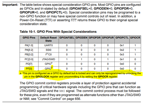
Part Number: EK-TM4C123GXL
I have a project that I'm using the EK-TM4C123GXL Launchpad on. I've got an LED connected to PF0 via the P2 header (Pin 4). When I laid out the PCB I missed that this gpio was used for the external wake on GPIO function of the launchpad. There is a pullup on the launchpad connected to USER SW2 (pushing the switch shorts to GND and pulls the WAKE pin down. ) When I realized this, I looked at the schematic of the launchpad and it looks like there is a 0 Ohm resister, R1, that connects PF0 to the pull-up and switch. So, I removed R1 from the Launchpad, but Pin 4 is still always logic HIGH. I'm using PF1 for a second LED that works fine. The code is the same for both (using the DRV LIB to configure as an output and then GPIOPinWrite() to set the state. As I said, the LED on PF1 works fine and when R1 was still connected, I could push USR SW2 and the LED would go out. (I've got he LED on a MOSFET), so there is a 5V pullup on the gate side which is connected to the PF0 output.
Is the published schematic correct for the EK-TM4C123GXL? Is R1 the correct jumper to remove?