This thread has been locked.

If you have a related question, please click the "Ask a related question" button in the top right corner. The newly created question will be automatically linked to this question.

CCS/TMS570LS1224: TMS570LS12x MCP4922 SPI Communication

Part Number: TMS570LS1224
Other Parts Discussed in Thread: HALCOGEN

Tool/software: Code Composer Studio

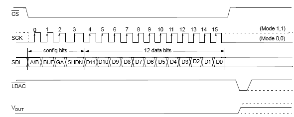
This is the Device SPI register;

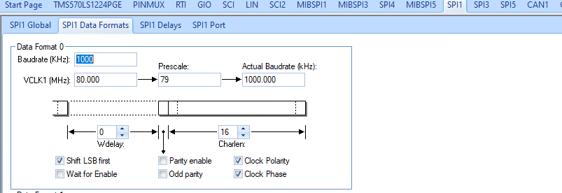
This is the halcogen part;

And the last one this is the code 

#include "sys_common.h"
#include "sys_core.h"
#include "spi.h"

/* USER CODE BEGIN (1) */
/* USER CODE END */

/** @fn void main(void)
*   @brief Application main function
*   @note This function is empty by default.
*
*   This function is called after startup.
*   The user can use this function to implement the application.
*/

/* USER CODE BEGIN (2) */
uint16 TX_Data[] = {0xF7D0};
uint16 RX_Data[] = {};
/* USER CODE END */

int main(void)
{
/* USER CODE BEGIN (3) */
    spiDAT1_t dataconfig1_t;

    dataconfig1_t.CS_HOLD = FALSE;
    dataconfig1_t.WDEL = TRUE;
    dataconfig1_t.DFSEL = SPI_FMT_0;
    dataconfig1_t.CSNR = 0xFE;


    spiInit();

   spiSendData(spiREG1, &dataconfig1_t, 16, &TX_Data);

   spiSendAndGetData(spiREG1, &dataconfig1_t, 16, &TX_Data, &RX_Data);
    while(1)
    {

    };
/* USER CODE END */

    return 0;
}

so nothing happen in the DAC part. Can anyone help me ?

  • Hello Suat,

    From the first SPI timing diagram, the SDI is MSB first. But the "Shift LSB first" is checked in your SPI configuration. Please also double check the requirement of clock phase and polarity on the SPI device (DAC) datasheet.

  • Hello Wang;

    Thanks for advising I double checked clock phase and polarity and the circuit works with mode 11 and 00 so I tried 00 and 11 but still I couldn't find the problem 

    In the dataconfig part there is DFSEL and CSNR exist and I couldnt find any explanation about them can you help me?

  • Hello,

    Have you tried the MSB for SDI?  MSB means that the most significant BIT is sent out first. This means bit15 - bit14 - bit14....bit1, bit0 of a 16-bit word.

    LSB reverses the transmission order: bit0 - bit1 - bit2....bit14, bit15 of a 16-bit word.

    DFSEL: Data word format select.. Four independent data word formats are supported for different types of slaves in one SPI network. The data word formats are configured through SPIFMTx registers.

    CSNR: Chip select (CS) number which defines the chip select pins that will be activated during the data transfer. If you use SPICS[0], 0xFE should be written to CSNR field. The default value of each chip select (not active) can be configured via the register CSDEF.

  • Hello,

    Yes I figure out that I senf them in the wrong direction it has to be MSB. I did it just after upload this post. So I tried everything you said and doesn t work so i write a code it acts like SPI but I manupilated the  GPIOs and worked correctly. 

    In the conclusion I couldnt start well the SPI module of the TMS but I write a SPI code which works on GPIOs.

  • I noticed that you called the SPI API incorrectly. 

       spiSendData(spiREG1, &dataconfig1_t, 16, &TX_Data);
       spiSendAndGetData(spiREG1, &dataconfig1_t, 16, &TX_Data, &RX_Data);
    16 is the block size. But the array size TX_Data() and RX_Data() in your declaration is 1.