


Part Number: TM4C1294KCPDT
Hi,
In our application, we are using M12 (4-pin ) connector for Ethernet connectivity. As per standard pin configuration of M12 connector, all signals routing in top layer is not possible, so 1 signal routed in 2 different layer through VIA. As per guidelines all signals routing should be in top layer without any VIA .
As the layout revision is going on, please advise best possible way to route Ethernet signal.
Existing routing details:
- TX_N, RX_P & RX_N : Routed in top layer
- TX_P : Routed in top & inner layer
- differential spacing not tuned to the PCB stack-up for 100Ω differential impedance.
- 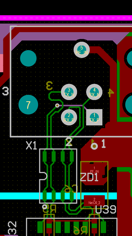 Only differential routing & length matching done.
Please refer attached layout image for reference & suggest the solution to improve layout ASAP.
Thanks,
Tusarkanta Das

