This thread has been locked.

If you have a related question, please click the "Ask a related question" button in the top right corner. The newly created question will be automatically linked to this question.

CCS/RM46L852: OTP programming

Part Number: RM46L852

Tool/software: Code Composer Studio

Hi,

I am working with the TI RM46L852  device and I need a clarify how to program the OTP part of the flash memory. I program the flash memory and EEPROM using F021 Flash API, version 2.01.01. I can succesfull erase/program BANK0 flash(0x0 - 0x13_FFFF) and BANK7 EEPROM flash(0xF020_0000 - 0xF020FFFF). Now I study the possibilities of programming the OTP memory and I have some questions. I will be very grateful for answers to the next questions:

1. The device memory map table(6.9.2) in the datasheet illustrate that two OTP memory ranges are used. First, the TCM Flash Banks OTP is for Bank 0 and second for Bank 7. Am I right? Or there is only one OTP memory?

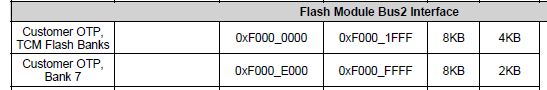
2. Does the picture above means, that TCM FLash Banks OTP sets the security rule for BANK0 flash and OTP Bank7 for EEPROM? 

3. Is the OTP memory intend for general purpose or have some special meaning, i.e. some OTP memory bytes have special meaning? If yes, where can I find the description of the memory? 

Next questions will belongs to the code developing in CCS:

4. The Reference guide for the F021 Flash API (spnu501G) talks about function Fapi_enableBanksForOtpWrite(uint8_t u8Banks). The "u8Banks" parameter indicate the bank to be enabled. So, does it means that for programming the TCM flash banks(0xF000_0000 to 0xF000_1FFF) is needes to use the u8Banks = 0x1(1 shl 0) and for Bank 7 OTP(0xF000_E000 to 0xF000_FFFF) the u8Banks = 0x80(1 shl 7)?

5. Is this the following algo steps for programming the whole OTP TCM flash banks(0xF000_0000 to 0xF000_1FFF) right? Algo:

oReturnCheck = Fapi_initializeFlashBanks(220);
if(oReturnCheck != Fapi_Status_Success) {
    break;
}
oReturnCheck = Fapi_setActiveFlashBank(Fapi_FlashBank0);
if(oReturnCheck != Fapi_Status_Success) {
    break;
}
oReturnCheck = Fapi_enableBanksForOtpWrite(0x1);
if(oReturnCheck != Fapi_Status_Success) {
    break;
}
oReturnCheck = Fapi_issueProgrammingCommand((uint32 *)(0xF0000000),(uint8 *)Buffer+i,8,0,0,Fapi_AutoEccGeneration);
if(oReturnCheck != Fapi_Status_Success) {
    break;
}
oReturnCheck = Fapi_disableBanksForOtpWrite();
if(oReturnCheck != Fapi_Status_Success) {
    break;
}

6. Is the same steps as in algo above also valid for Bank7 OTP programming, with the difference of using Fapi_setActiveFlashBank(Fapi_FlashBank7) and Fapi_enableBanksForOtpWrite(0x80)?

Thanks for help!

Best regards,

Tomas

  • Hello, 1. The flash contains the program flash (bank 0), data flash (EEPRO, bank7), and one customer OTP sector and one TI OTP sector per bank. There is only one OTP memory, but it consists of several sectors (customer OTP sectors, TI OTP sector). 2. The customer OTP sectors is programmed by the customer, but can not be programmed. The TI OTP sectors contain manufacturer information, for example TI OTP has settings used by flash API to setup the flash state machine. The AJSM key are stored at the first 128-bit of customer OTP sector (0xF0000000). Please refer to OTP memory sector in TRM. 3. OTP (one-time programmable): A program-only-once Flash sector (cannot be erased). Please refer to section of OTP Memroy in TRM. 4. It is bit mask, and each bit corresponds to a Flash bank. Bit 0 (0x01) is for bank0, and bit 6 (0x40) for bank 7. 5. Correct. Please be aware of that the OTP is one-time programmed only, and cannot be erased. 6. yes, same procedure for bank 7.
  • Hi,

    your answer helps, but I am still a little bit confused... I understand that OTP means one-time programmable memory which cannot be erased. I need to clarify:

    1. You said, that there is only one OTP memory, but consist of several sectors. I don't understand your sentence - "2. The customer OTP sectors is programmed by the customer, but can not be programmed.". So how can I program it, if I can't as you said? What do you mean by this sentence?

    2. What is the complete and correct address range for OTP memory which can user program?

    3. Can I program only memory ranges from 0xF000_0000 to 0xF000_0FFF (4kB of memory)? Or also memory range from 0xF00E_0000 to 0xF00E_07FF (2kB of memory)?

    4. I understand that first 128bits of OTP contains AJSM keys. I try to program the rest of OTP memory (address range from 0xF000_0010 to 0xF000_0FFF) with random values, everything works fine. Am I able to program also the AJSM keys location in the same way as the rest of OTP memory locations(the code showns above in  point 5)? Or programming this locations need some special access?

    Thanks for help!

    Best regards,

    Tomas

  • Hello Tomas,

    1. Sorry for my type. It should be "can not be erased".

    2. The customer OTP for bank0: 4KB, 0xF0000000 ~ 9xF0000FFF

         customer OTP for bank 7: 2KB, 0xF000E000~0xF000E800

    3, Yes, it is 4KB and 2KB,

    4. You can use the same way to program 0xF00000000~0xF000000C (AJSM key locations). Please write down the key before you write it to 0xF0000000. Once the JTAG is locked, the target can not be connected through JTAG with providing the unlock key. 

  • Hi,

    thank you for your support. I am able to program the OTP memory.

    But I have find out that the parameter "u8Banks" for Fapi_enableBanksForOtpWrite(uint8_t u8Banks) function needs to have the parameter 0x80 for Bank7. Not the 0x40(as you said). The 0x40 parameter don't program the OTP Bank7 locations 0xF000E000~0xF000E800.3

    This thread can be now closed.

    Thank you!

    Best regards,

    Tomas