This thread has been locked.

If you have a related question, please click the "Ask a related question" button in the top right corner. The newly created question will be automatically linked to this question.

TM4C123GH6PM: Trouble with precise pin timing on TivaC (dShot protocol)

Part Number: TM4C123GH6PM

I'm attempting to add support for a pseudo digital protocol to a project of mine. I'm attempting to implement the dShot protocol for controlling ESCs on my thrust stand, and having some issues. The TivaC doesn't appear to have very robust output control. You can see what I'm trying to do here:

Basically the protocol uses a modified PWM signal with each bit being 1.67us period with 1250ns representing a 1 and 635ns representing 0, basically encoding a 2048 bit throttle signal with some CRC data and a telemetry call bit crammed on the ends. After a couple days I've gotten to the point of using a PWM timer synced with a GP timer to attempt to modify the duty cycle for each bit, however I'm not having much luck.  Is there a more precise way of accomplishing this? I'd like to not have to switch MCUs, but I know the ESP32 can do this easily with their RMT methodology and the STM chips can do with with a DMA transfer.  I looked at the uDMA implementation in the TivaC and it doesn't appear to operate in a way that would work to toggle pins like this.

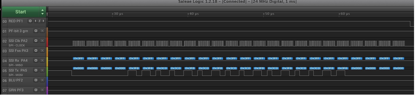
This is the output signal I'm getting on my relatively limited DSO Nano from the TivaC:

And this is the output signal as seen from an STM32F405 that is working properly:

Any help would be very much appreciated.

  • Hi Ryan,

      First of all, I have to say I have no knowledge about Dshot protocol. I have looked at your code.

      Can you explain the relationship between TIMER1 which you use as a PWM and PWM_GEN_2 and PWM_GEN_3 of the PWM0 module? Do these three PWM signals need to be synchronized to each other.

      I only see you enable the locally-synchronize as in PWM_GEN_MODE_SYNC for the PWM_GEN_2 and PWM_GEN_3? Do you need to synchronize between PWM_GEN_2 and PWM_GEN_3? If you do, you need to try PWM_GEN_MODE_GEN_SYNC_GLOBAL so different PWM generators are synchronized to each other. 

      If there is a requirement to synchronize between TIMIER1 and the PWM0 module then there is not a way to do it. You will need to use another PWM generator in place of theTIMER1 for generating PWM signal. 


  • Hi Charles, sorry for the confusion, the PWM_GEN outputs are for the analog output portion of the code, and I haven't fully updated it yet. For now I'm focusing only on the primary motor output working with the digital protocol, then I'll update the other outputs.  I couldn't figure out how to get the PWM module to sync externally to non-pwm module timers, so I switched output 1 to a GP timer in PWM mode so I could sync it with the dshot bit progression timer. Regardless, even with it synced via the GP timers, it doesn't appear to output a consistent signal, and this is where I'm struggling. It seems that I'm not able to update the PWM duty cycle fast enough to have a it correct in time for the next timer cycle. At least that's how I'm reading it.

  • Hi Ryan,

      Excuse my ignorance on the dshot stuff. This is totally new to me.

      Is a PWM cycle equal to one dshot bit? 

      What is the period of a PWM?

      I'm still not clear which module you are using for your dshot generation? Is it the TIMER1 or the PWM_GEN_2 or PWM_GEN_3?

      What trigger your application to do a duty cycle update? Are you doing it in a context of the interrupt?

      Normally, you would update the duty cycle synchronized to the edge of the PWM. This is why you will need the PWM_GEN_MODE_SYNC flag. With that said, it means that you can have only one duty cycle update per PWM cycle. If you are trying to update more than once within a PWM cycle then the second update will overwrite the first update. So the question is how fast are you updating the duty? Is this duty cycle update somehow synchronized to the frequency of the PWM cycle?


  • Sure no worries, 

    Yes, one PWM cycle equals one bit for DShot. The period is 1670ns (1.67ms).

    In my code Timer1A is the timer for the PWM DShot output, and Timer 4A is the timer that updates the PWM duty cycle once each cycle. I've synced Timer4A and Timer1A with Timer1 as the reference to try to make sure that the updates happen in sync. I'm attempting to update duty cycle exactly once each cycle based on an array of duty cycle values representing each bit in the 16bit packet.

  • Hi Ryan,

     Thanks for the explanation. 

      What is the relationship between ADC and timer1A? I see below code. Why are you not clearing the Timer1A interrupt flags in its own Timer1A ISR but rather in the ADC ISR? I see various timers and PWM you use throughout the code. If TIMER1A and TIMER3A are what is critical as far as your current problem is concerned, can you for experiment purpose try to keep it simple by leaving out the rest of code (.e.g. remove ADC, TIMER5, PWM_GEN_2, PWM_GEN_3 and etc). Perhaps create a new test with just the TIMER1A and TIMER3A. Once you can resolve the current issue, you can gradually add other features one at a time. 

    void adcIntHandler() {
    TimerIntClear(TIMER1_BASE, TIMER_TIMA_TIMEOUT);
  • yeah that was a mistake, i fixed it. :D I switched the ADC to timer 5. That's just a timer to updated the stored ADC values. I overwrote the timer settings further down the code, so it didn't impact the DShot code, but the ADC variables weren't updating. 

    I'm really wishing i had a better scope right now! This DSO Nano doesn't have enough resolution to really see what's happening with the timings. 

  • I got my hands on a good scope at work, and have been able to do a good bit of debugging. I discovered that using T1CCP0 in PWM mode, zero PWM never really goes to full zero. I'm still getting a short tick at the beginning of every duty cycle. If I switch the mode to the actual PWM peripheral then I don't get that tick, it does go to a full off state at zero duty cycle. However now I have the issue of syncing the dutycycle updates so I get one update per PWM period. I'm getting enough jitter in the signal that it is not passing the CRC checks, and the longer it goes, the more out of sync it seems to get.  Is there another way to accomplish what I need?  Once again here is the protocol document. Any ideas on implementation would be extremely helpful. https://blck.mn/2016/11/dshot-the-new-kid-on-the-block/

  • Hi Ryan,

      I'm not surprised that you can't get to 0% duty cycle using TIMER module. You may even encounter problem with 100%. The 0% and 100% are always tricky and I vaguely remember so people reporting not getting 0 and 100%. If you can get the PWM to work using the actual PWM module then please stay with the PWM module instead of the TIMER module. 

      Have you used the PWM_GEN_MODE_GEN_SYNC_LOCAL flag when configuring the PWM with the PWMGenConfigure()? Please refer to the local sync mechanism as follows. 

  • Looking at the dshot protocol description, specifically how a BIT CELL is defined, there can be another way to make Tiva output dshot 0's and 1's using the SSI peripheral.

    If the SSI is set up in 8 bit mode to output a single character bit pattern like 11111100 binary, this would look like a dshot ONE bit as viewed on a scope.    Outputting a 11000000 pattern would look like dshot ZERO.

    That's one bit.  

    Now, to send out 16 dshot bits means that the SSI should send out 16 such character patterns.  (Is a dshot frame 16 bits? ).

    Sending out a dshot frame of 16 bits means creating a buffer of data & crc, then transmitting that buffer out the SSI.

    About clock rates, dshot maximum bit rate is 600kbps, this gives the 1.667 uSec cell size. So one possible clocking strategy can be:

    - tiva sysclock is set to 60mhz, and sent to SSI

    - SSI divides by 10 to give SSI clock of 6 mhz

    - use 10 bit characters to depict a dshot bit. This means one character comes out of SSI Tx at a 600kbps rate.

    - select one of the Motorola SPI bit protocols in the SSI setup

    The Tiva SSI peripheral should be ideal for this function as it :

    - has a 16 character FIFO

    - has variable length characters (10 in the example above)

    - has DMA capability, if needed for speed, to empty that 16 character buffer.

    Hopefully, this concept is useable.

    This idea to create zero/one bit cells using SPI/ SSI is nothing new.

  • Here is the timing off a Tiva code snippet:

    As usual, 'the devil is in the detail', so here are changes from the previous post:

    - 50 MHz sysclock was used as I could not find 60 MHz. This is OK since 50M / 12 gives the 6 MHz SSI clock.   Thus dshot 600KHz is shown.

    - the dshot ONE bit high time is 1.125 uS.       ZERO bit high time is 0.66 uS.      Both can be trimmed by changing the bit patterns.     In this example, SPI decoded as 0x3F8 is the dshot ONE bit cell.    Decoded as 0x3C0, the dshot ZERO.     For example, to shorten the high-time of dshot ZERO by some nano seconds, use the character 0x380.

    - the SSI Tx PA5 (trace channel 05, above, green) starts and ends at a high logic level; I do not know why nor did I attempt to investigate.  Instead, the 16 bit dshot frame was padded with four 'zero patterns' before and after sending the frame.   If necessary, I guess PA5 can be programmed back to GPIO in the inter-frame time period, but I did'nt check that detail.    The TI guys on this forum are amazing, so feel free to comment.

    - The SSI FIFO is 8 characters deep, not 16 as mentioned in the previous post.

    - since the frame goes out 'reasonably quickly', the code for this includes a technique to make is atomic so that the dshot frame is contiguous from SSI Tx PA5.

    I know this is not what you originally set out to do, so I hope this is useful and fits your bill !        (your last message:  "Any ideas on implementation would be extremely helpful." )

    Code snippet to follow ........

  • //*****************************************************************************
    //
    //      dshot protocol via tiva SSI     CCS v10     driverlib  2.2.0.295, the newest, Apr 2020
    //      ======================================================================================
    //
    //      - bit cell
    //      - dshot frame
    //      - information comes from :     blck.mn/.../
    //
    //      DSHOT           - 16 bit frame:  11 data,  1 status, 4 crc
    //                      -  TODO  the Fss / CS brackets each dshot bit cell, adds time - is this critical?
    //                      -  TODO
    //                      - repetition rate:  32KHz.   +- 3 mSec in this code snippet
    //
    //      Tiva clocking:  - sysclock 50MHz
    //                      - SSI clock 6MHz   (sysclock div 12, should come from SS0 API)
    //                      - dshot bit cell divided into 10 slices due to 10-bit SSI character
    //
    //      BIT CELL:       - ONE bit       11.1111.1000        0x03f8     (tweak)
    //                      - ZERO bit      11.1000.0000        0x0380     (tweak)
    //
    //      SSI0 peripheral - GPIO Port A peripheral (for SSI0 pins)
    //                      - SSI0Clk - PA2
    //                      - SSI0Fss - PA3
    //                      - SSI0Rx  - PA4
    //                      - SSI0Tx  - PA5
    //
    //      The dshot frame SSI routine has been made 'atomic / uninterruptable' - in this snippet
    //
    //*****************************************************************************
    
    #include <stdint.h>
    #include <stdbool.h>
    #include "inc/hw_types.h"
    #include "inc/hw_memmap.h"
    #include "driverlib/sysctl.h"
    #include "driverlib/interrupt.h"
    #include "driverlib/gpio.h"
    #include "driverlib/pin_map.h"
    #include "driverlib/ssi.h"
    
    
    #define RED_LED   GPIO_PIN_1        // LP pin PF1
    #define BLUE_LED  GPIO_PIN_2        // LP pin PF2
    #define GREEN_LED GPIO_PIN_3        // LP pin PF3
    
    #define ONE         0x03f8          //  11.1111.1000
    #define ZERO        0x03c0          //  11.1100.0000
    
        uint16_t    array [] =   { 0,0,0,0,                 // start the frame LOW  (HEADER)
                                   ONE, ONE, ZERO, ZERO,    // 16 bits/frame   *** TEST DATA HEREIN ***
                                   ONE, ZERO, ONE, ZERO,
                                   ZERO, ONE, ZERO, ONE,
                                   ZERO, ZERO, ONE, ONE,
                                   0,0,0,0                  // end the frame LOW (TRAILER)
                                    };
        uint32_t    ui32Index = 0;
        uint32_t    Frame = (sizeof array) / 2;             // number of characters to send = number dshot bits +1


    //*****************************************************************************
    //************     S T A R T   O F   M A I N     ******************************
    //*****************************************************************************
    int
    main(void)
    {
    
        //  ***********************************************************************
        // Setup the system clock to run at 50 Mhz from PLL with crystal reference
        SysCtlClockSet(SYSCTL_SYSDIV_4|SYSCTL_USE_PLL|SYSCTL_XTAL_16MHZ|
                        SYSCTL_OSC_MAIN);
    
    
        //  ***********************************************************************
        // Enable and wait for port F, set as output for LEDs
        SysCtlPeripheralEnable(SYSCTL_PERIPH_GPIOF);
        while(!SysCtlPeripheralReady(SYSCTL_PERIPH_GPIOF))
        {
        }
        GPIOPinTypeGPIOOutput(GPIO_PORTF_BASE, RED_LED|BLUE_LED|GREEN_LED);
    
        
        //  ***********************************************************************
        // Enable the SSI 0 peripheral
        //
        //  - set up the GPIO pins on Port A
        //  - set up the SSI 0
        //
        SysCtlPeripheralEnable(SYSCTL_PERIPH_GPIOA);
        GPIOPinConfigure(GPIO_PA2_SSI0CLK);                 // used only for monitoring via logic analyser
    //    GPIOPinConfigure(GPIO_PA3_SSI0FSS);                 // ditto, to unsure no FSS / CS activity
    //    GPIOPinConfigure(GPIO_PA4_SSI0RX);                  // not needed at att
        GPIOPinConfigure(GPIO_PA5_SSI0TX);                  // this is the DSHOT output stream, the only needed signal
        GPIOPinTypeSSI(GPIO_PORTA_BASE,
                       GPIO_PIN_5 | GPIO_PIN_2);
    //    GPIOPinTypeSSI(GPIO_PORTA_BASE,
    //                   GPIO_PIN_5 | GPIO_PIN_4 | GPIO_PIN_3 |
     //                  GPIO_PIN_2);
        //
        // Configure the SSI.
        //
        SysCtlPeripheralEnable(SYSCTL_PERIPH_SSI0);
        while(!SysCtlPeripheralReady(SYSCTL_PERIPH_SSI0))
        {
        }
        SSIConfigSetExpClk(SSI0_BASE, SysCtlClockGet(),
                           SSI_FRF_MOTO_MODE_0,
                           SSI_MODE_MASTER,
                           6000000,
                           10);
        //
        // Enable the SSI module.
        //
        SSIEnable(SSI0_BASE);
    
    
        //  ***********************************************************************
        //
        // Loop Forever
        //
        while(1)
        {
    
            bool bIntsOff;
            //
            // Turn interrupts off temporarily.
            //
            bIntsOff = IntMasterDisable();
    
    
            //
            // Turn on the RED LED to time the SSI transmission
            GPIOPinWrite(GPIO_PORTF_BASE, RED_LED|BLUE_LED|GREEN_LED, RED_LED);
            SysCtlDelay(200);
    
    
            //
            // Send the array 16 dshot bits = one dshot frame
            //
    
            for(ui32Index = 0; ui32Index < Frame; ui32Index++)
            {
                //
                // Send the data using the "blocking" put function.  This function
                // will wait until there is room in the send FIFO before returning.
                // This allows you to assure that all the data you send makes it into
                // the send FIFO.
                //
                SSIDataPut(SSI0_BASE, array[ui32Index]);
            }
    
            //
            // Wait until SSI0 is done transferring all the data in the transmit FIFO.
            //
            while(SSIBusy(SSI0_BASE))
            {
            }


            //
            // Turn off the RED LED
            GPIOPinWrite(GPIO_PORTF_BASE, RED_LED, ~RED_LED);
    
            //
            // Restore the interrupt state
            //
            if(!bIntsOff)
            {
                IntMasterEnable();
            }


            //
            // Delay for the next dshot frame
            SysCtlDelay(45000);                 // about 3 mSec
    
        }
    
    }   //********************************************************************
    //************     E N D  O F   M A I N     ******************************
    //************************************************************************
    

  • Thanks man! This is awesome, exactly what I'm looking for. I started adding DMA driven SSI to my code, but I still appreciate your example code. Thanks so much for your help on this!

    EDIT: Looks like uDMA is limited to 8 or 16 bit, no 10 bit, so not sure this will work. I wonder if I can do a 16 bit transfer at a faster clock speed? Maybe 16 bit at 9.6mhz?

    EDIT2: Nevermind, I misunderstood the DMA transfer methodology. It will DMA the 16 individual dshot cells, so the cells can still be 10 bit. Correct?

  • Ok, here's my code, let me know if I'm on the right track.

    void dshotOutput(uint16_t value, bool telemetry) {
        
        uint16_t packet;
        
        // telemetry bit    
        if (telemetry) {
            packet = (value << 1) | 1;
        } else {
            packet = (value << 1) | 0;
        }
    
        // github.com/.../pwm_output.c
        int csum = 0;
        int csum_data = packet;
        for (int i = 0; i < 3; i++) {
            csum ^=  csum_data;
            csum_data >>= 4;
        }
        csum &= 0xf;
        packet = (packet << 4) | csum;
    
        // durations are for dshot600
        // blck.mn/.../
        // Bit length (total timing period) is 1.67 microseconds (T0H + T0L or T1H + T1L).
        // For a bit to be 1, the pulse width is 1250 nanoseconds (T1H – time the pulse is high for a bit value of ONE)
        // For a bit to be 0, the pulse width is 625 nanoseconds (T0H – time the pulse is high for a bit value of ZERO)
        
        uint16_t steps = 0;
        while(dShotWriteActive == true){}   // Wait for dshot to finish writing
        for (int i = 0; i < 16; i++) {
          dshotPacket[i] = 0;
          
          if(i < 16) {
            if (packet & 0x8000) {
                // construct packet 1
                steps = 0x03f8;          //  11.1111.1000
            } else {
                // construct packet 0
                steps = 0x03c0;          //  11.1100.0000
            }
            dshotPacket[i]= steps;
            packet <<= 1;
          }
        }
       return;
    
    }
    
    uint8_t update_crc8(uint8_t crc, uint8_t crc_seed){
      uint8_t crc_u, i;
      crc_u = crc;
      crc_u ^= crc_seed;
      for ( i=0; i<8; i++) crc_u = ( crc_u & 0x80 ) ? 0x7 ^ ( crc_u << 1 ) : ( crc_u << 1 );
      return (crc_u);
    }
    
    uint8_t get_crc8(uint8_t *Buf, uint8_t BufLen){
      uint8_t crc = 0, i;
      for( i=0; i<BufLen; i++) crc = update_crc8(Buf[i], crc);
      return (crc);
    }
    
    
            SysCtlPeripheralEnable(SYSCTL_PERIPH_SSI2);
            while(!SysCtlPeripheralReady(SYSCTL_PERIPH_SSI2)){}
            
            SysCtlPeripheralSleepEnable(SYSCTL_PERIPH_SSI2);
            
            //
            // Configure GPIO Pins for SSI2 mode.
            //
            GPIOPinConfigure(GPIO_PB7_SSI2TX);
            GPIOPinTypeSSI(GPIO_PORTB_BASE, GPIO_PIN_7);
        
            SSIConfigSetExpClk(SSI2_BASE, SysCtlClockGet(), SSI_FRF_MOTO_MODE_0,
                    SSI_MODE_MASTER, 6000000, 10);
        
            SSIEnable(SSI2_BASE);
    
            //****************************************************************************
            //uDMA SSI2 TX
            //****************************************************************************
        
            //
            // Put the attributes in a known state for the uDMA SSI2TX channel.  These
            // should already be disabled by default.
            //
            uDMAChannelAttributeDisable(UDMA_CHANNEL_SSI2TX,
                                            UDMA_ATTR_ALTSELECT |
                                            UDMA_ATTR_HIGH_PRIORITY |
                                            UDMA_ATTR_REQMASK);
        
            //
            // Set the USEBURST attribute for the uDMA SSI2TX channel.  This will
            // force the controller to always use a burst when transferring data from
            // the TX buffer to the SSI2.  This is somewhat more effecient bus usage
            // than the default which allows single or burst transfers.
            //
            uDMAChannelAttributeEnable(UDMA_CHANNEL_SSI2TX, UDMA_ATTR_USEBURST);
        
            //
            // Configure the control parameters for the SSI2 TX.
            //
            uDMAChannelControlSet(UDMA_CHANNEL_SSI2TX | UDMA_PRI_SELECT,
                                      UDMA_SIZE_16 | UDMA_SRC_INC_16 | UDMA_DST_INC_NONE |
                                      UDMA_ARB_4);
        
        
            //
            // Set up the transfer parameters for the uDMA SSI2 TX channel.  This will
            // configure the transfer source and destination and the transfer size.
            // Basic mode is used because the peripheral is making the uDMA transfer
            // request.  The source is the TX buffer and the destination is the SSI2
            // data register.
            //
            uDMAChannelTransferSet(UDMA_CHANNEL_SSI2TX | UDMA_PRI_SELECT,
                                                           UDMA_MODE_BASIC, dshotPacket,
                                                           (void *)(SSI2_BASE + SSI_O_DR),
                                                           16);
        
            //
            // Now the uDMA SSI2 TX channel is primed to start a
            // transfer.  As soon as the channel is enabled, the peripheral will
            // issue a transfer request and the data transfer will begin.
            //
            uDMAChannelEnable(UDMA_CHANNEL_SSI2TX);
        
            //
            // Enable the SSI2 DMA TX/RX interrupts.
            //
            SSIIntEnable(SSI2_BASE, SSI_DMATX);
        
            //
            // Enable the SSI2 peripheral interrupts.
            //
            IntEnable(INT_SSI2);
    

    The next thing is I have an interrupt cycling at the update rate (rate at which I'd like to send dshot packets. Now I need to figure out how to move the DMA execution code into the interrupt so it only fires the DMA transfer once per interrupt. 

  • I updated the full code base on github. It compiles but I'm not getting any output on the pin yet.  https://github.com/VirtualEnder/TestStandv2/blob/dev/MQTB_Thrust_Stand/hardwareTimers.ino

  • Hi Ryan,

      I hope you find the example by Otto useful. Please let us know your status and if we can close the thread.