This thread has been locked.
If you have a related question, please click the "Ask a related question" button in the top right corner. The newly created question will be automatically linked to this question.
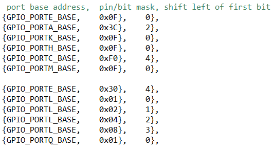
I have to modify some code someone else wrote but I'm a little confused about how things work since it says there are 15 different blocks corresponding to an individual GPIO port and then looking down, the datasheet has 43 different GPIO registers with offsets that show the 15 ports.
Here is the code I'm trying to modify. One of the things I especially don't understand is the shift left of the first bit as well so can someone please help me understand it better so I'm able to modify it.
Hi,
You are showing a snippet of code with no context of what/how it is used for. I will suggest you contact the person you got the code from and ask what his comment is about. Only he/she knows what is the intention of doing the mask and then the shift.
My best guess is the code is trying to write to individual pins but I don't know for sure. See if the below Data Register Operation makes sense to you in relation with the code you got. Again, you should check the code author or at least you need to provide the full context like what functions are being used to act these elements.
Sorry, only the original author of the code knows what his intention is. The code looks very application specific. I really don't know for sure what is going on. As I said, my best guess is that he is try to control a specific bit(s) of a port. For example the {GPIO_PORTE_BASE, 0x0F) means that he is going to control/write the bits 0,1,2,3,4 of the Port E. Look at the {GPIO_PORTC_BASE, 0xF0}, 4}, the 0xF0 is 11110000. His last argument is a 4. It seems like he is doing some type of masking of either the first four or the last four bits. I don't know for sure. You really need to ask the author. This is really not a question I can help with. I don't know where to start.