


Part Number: TMS570LC4357
Other Parts Discussed in Thread: HALCOGEN
Hi,
I'm currently working with the EMIF of the TMS570LC4357 MCU. I'm interfacing an external FPGA which exposes a bank of registers that are in turn mapped onto the Async1 address range of the EMIF block (0x60000000~0x64000000). The FPGA performs a set of operations towards different peripherals based on specific commands and data that are passed to it through the exposed registers and it in fact acts as an asynchronous memory for what may concern the EMIF. All the FPGA registers are 16 bit width, thus each R/W access through the EMIF is 2-byte based.
Current settings of the MCU's EMIF are:
PLL = 300 MHz
VCLK3 = 150 MHz (EMIF_CLK)
EMIF read setup/strobe/hold = 14 /48 / 2 (ECLK)
EMIF write setup / strobe / hold = 14 / 14 / 2 (ECLK)
EMIF turnaround = 1 (ECLK)
So far everything works as expected, nevertheless during a recent test I found the following issue. The FPGA is connected, among other devices, to a NAND Flash: a specific register, the command register, (@ 0x60800000) is reserved to receive the command for the NAND Flash (write a page, read a page and so on) while another one, the status register, (@ 0x60800002) is used to check if the FPGA's Flash controller is either busy or idle. In particular, sending the "write page" command (writing 0x8000 to 0x60800000) will immediately trigger the FPGA state machine which goes into the busy state and will set the busy bit of the status register (I should read 0x0001 from 0x60800002). For this reason, after setting the "write page" command, I read the status register and wait for it to become idle again (back to 0x0000). The first step is to set the address of the NAND Flash page I want to write, so that I use another pair of FPGA registers for this purpose ("low address" and "high address") at 0x60800004 and 0x60800006. So the C code is as follows:
*((volatile uint16_t *) 0x6080004) = BUILD_LOW_ADDRESS(block, page, column);
*((volatile uint16_t *) 0x6080006) = BUILD_HIGH_ADDRESS(block, page, column);
*((volatile uint16_t *) 0x6080000) = 0x8000U;
while (*((volatile uint16_t *)0x60800002) != 0) {
// Handle a timeout
}
I also paste in the following the Assembly code snippet of the sequence I wrote for this operation:
// Various arithmetic operations to build the low address value
ldr r2, [pc, #156] ; <--- Load into R2 the low address register's address (0x608000024is written in the .text section at this offset)
strh r3, [r2, #0] <--- Write the low address register
// Various arithmetic operations to build the high address value
ldr r3, [pc, #160] <--- Load into R3 the high address register's address (0x60800006 is written in the .text section at this offset)
strh r4, [r3, #0] <--- Write the high address register
mov.w r2, #32768 ; 0x8000 <--- Write the "write page" command to R2
mov.w r3, #1619001344 ; 0x60800000 <--- Write the command register's address to R3
strh r2, [r3, #0] <--- Store the command into the command register
ldr r2, [pc, #132] <--- Load the status register's address into R2 (0x60800002 is written in the .text section at this offset)
ldrh r3, [r2, #0] <--- Read the status register's content
Nevertheless, I've noticed that, no matter what, there's no way I could see the "busy" state of the status register and every time the FPGA looked like idle, so that I proceed with the Flash programming but it unavoidably fails. So I tried to look at the busy bit transitions with the oscilloscope and I found the following:
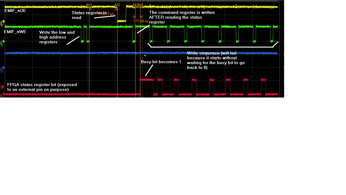
It looks like the EMIF hardware swaps the order of the code flow by reading first the status register and then writing the command register. According to the TMS570LC43x Technical Reference Manual, section 21.2.13, an asynchronous read's priority is higher than the corresponding write and I was wondering if, since the hardware "may think" that there cannot be any data hazard in the two R/W instructions (the access is two byte so that there's no overlap and they involve different "SRAM-like" addresses), this kind of event may indeed happen.
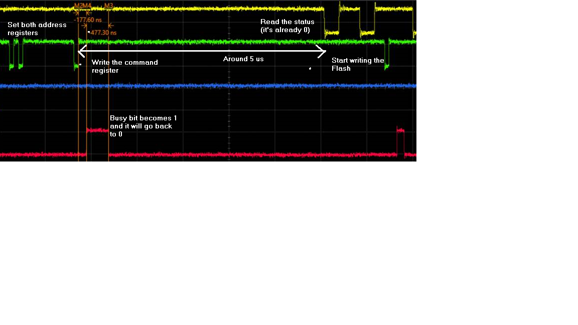
Adding an artificial delay between writing the command register and reading the status register will instead make the sequence go as expected:
Is this behavior normal?
Thanks in advance for any suppport.
