Part Number: TM4C129ENCPDT
Other Parts Discussed in Thread: EK-TM4C1294XL
Tool/software: TI C/C++ Compiler
Hi,
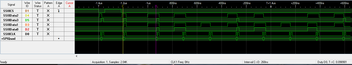
I' working with the DK-TM4C129X on the Quad-SPI Flash, where I could find the same problem as in my "real" target hardware.So I'm referring to the DK and there usb_dev project, as this can be easier cross-checked. The example usb_dev etc. works, but when I look into the details, I found that the MX66L51235FRead() functions does only use single-SPI.
I changed the MX66L51235FRead() and the reading ROM function from
ROM_SPIFlashRead(SSI3_BASE, ui32Addr, pui8Data, ui32Count);
to
ROM_SPIFlashDualRead(SSI3_BASE, ui32Addr, pui8Data, ui32Count);
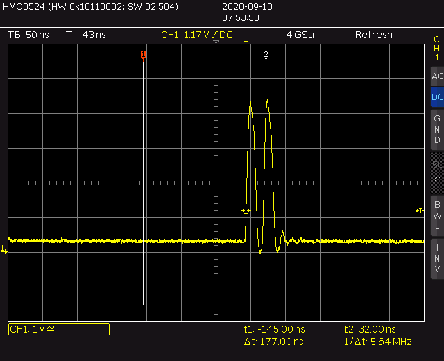
which still runs. I checked the oszilloscope and saw the 2xtimes Outputs as expected. But when using
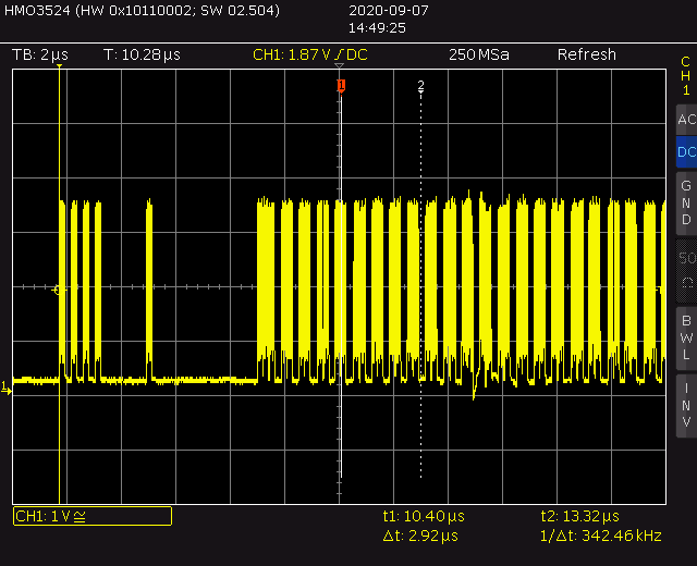
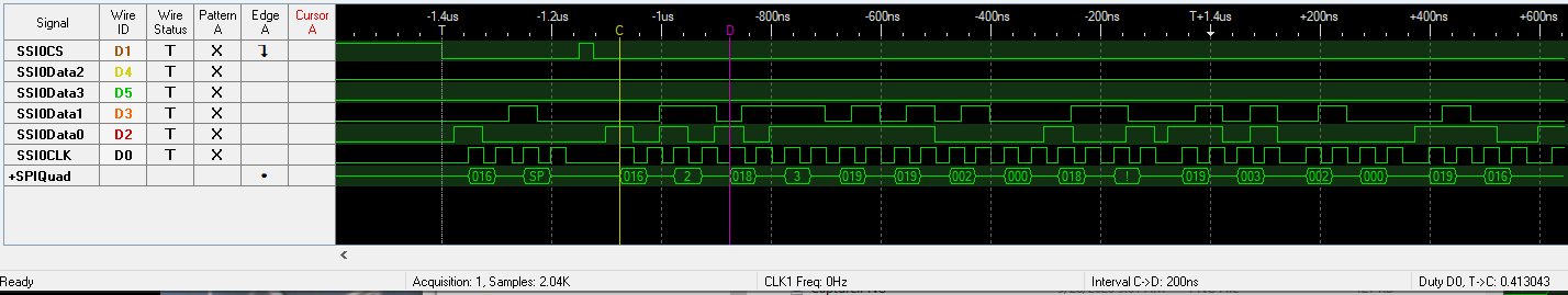
ROM_SPIFlashQuadRead(SSI3_BASE, ui32Addr, pui8Data, ui32Count);
the result is obviously wrong. Do I have to consider something special or is there something missing?
Thanks in advance
Micky