This thread has been locked.

If you have a related question, please click the "Ask a related question" button in the top right corner. The newly created question will be automatically linked to this question.

CCS/TM4C1294NCPDT: TM4C1294NCPDT Ethernet link sometimes doesn't get established.

Part Number: TM4C1294NCPDT
Other Parts Discussed in Thread: TPD4E1B06, ESDS314

Tool/software: Code Composer Studio

I am having an issue with a custom board that we have developed using the TM4C1294NCPDT. I have used the chip before but have never used it for an Ethernet connection, I was able to get some proof of concept code working on the launchpad, and was then able to get it working OK on my custom board.

However later discovered an issue that didnt appear to show up at all when I was doing my initial development, sometimes when the board is powered on the ethernet link is either very slow to establish or never establishes.

I can generally get the link to connect by waiting 30 seconds to see if the link gets establish, if it doesn't I hit the hardware reset button and try again.

If the link is established, and then a connection to our other controller is established the link seems to be pretty reliable and hasn't dropped out even when left powered on overnight.

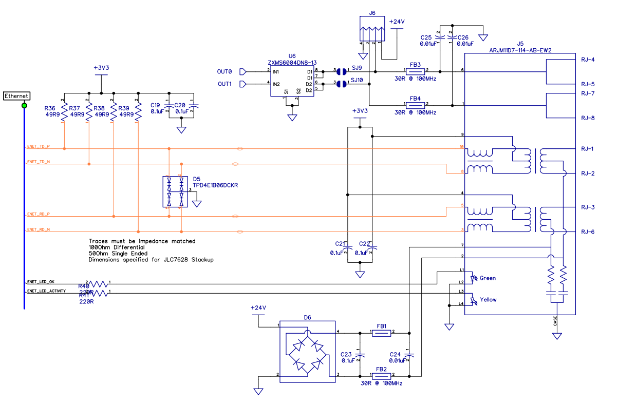
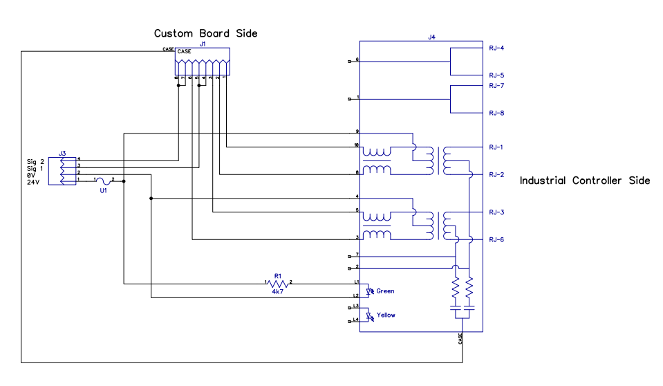
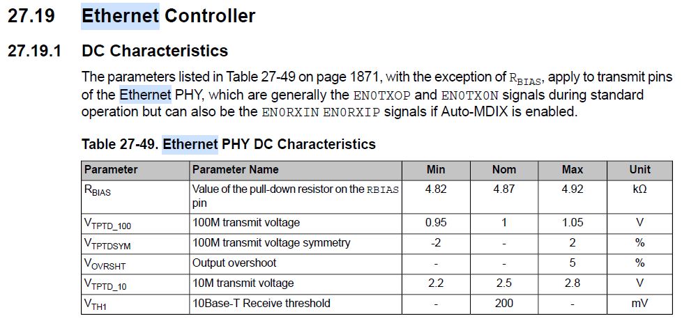
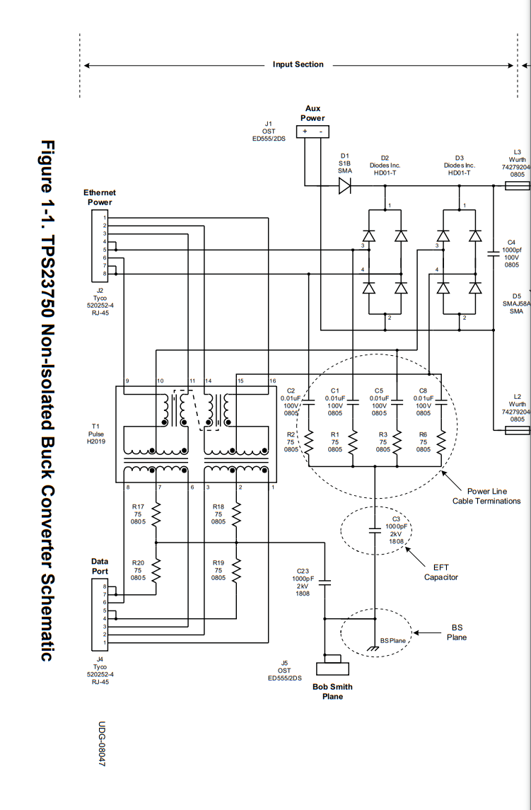
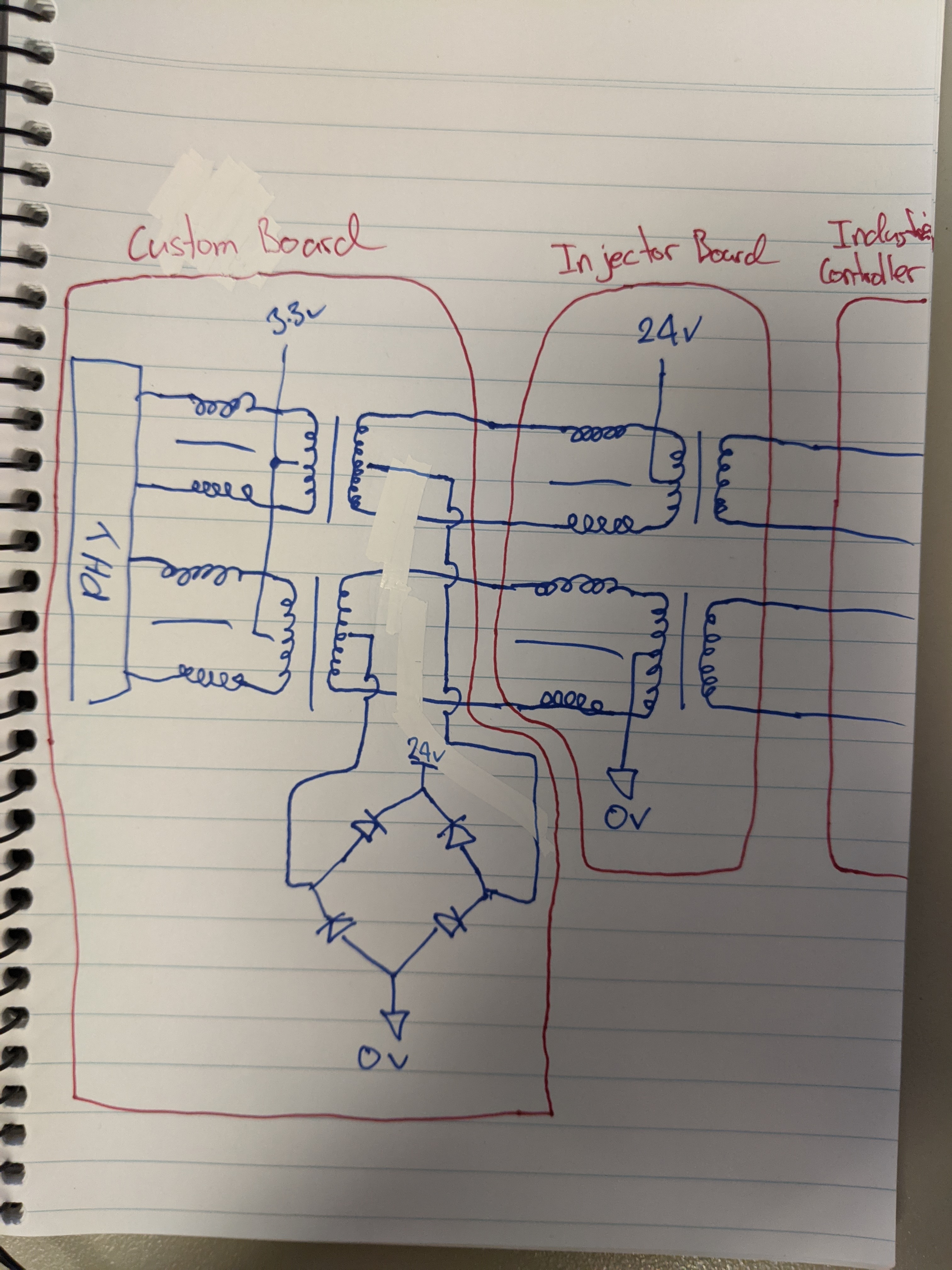
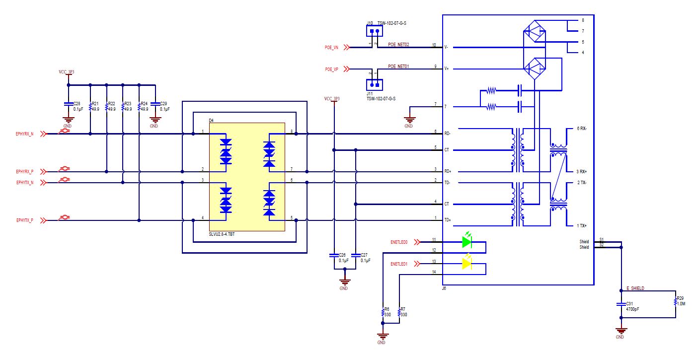
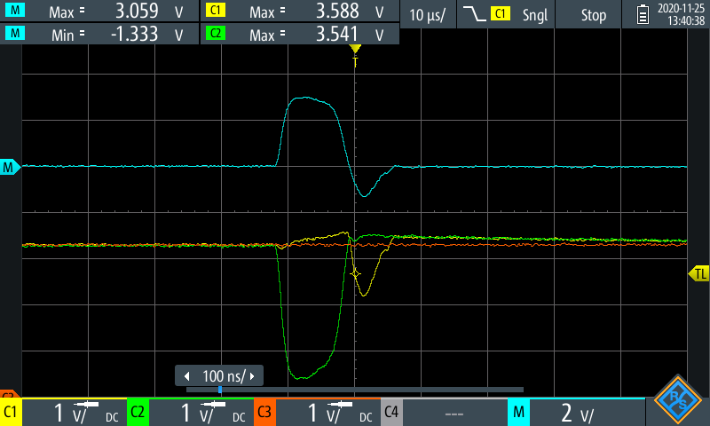
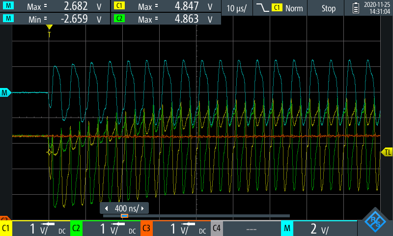
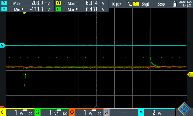
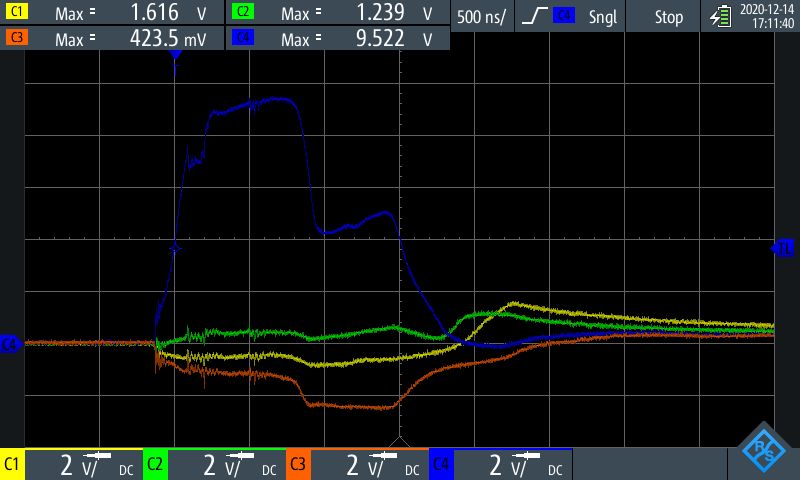
I have followed the TI guidelines on the Ethernet connection with the exception that the pairs are also used for power supply and some very slow digital signals, for the purposes of this testing none of these signals are switching and are held to one supply rail or the other. The result of this is that the signal path between the TM4C and the industrial controller effectively has 3 sets of magnetics instead of the usual two. One on the board with the TM4C as per TI recommendations, one in the middle where power and signals are injected, and one in the industrial controller. I am aware the extra set of magnetics is introducing losses into the system however the cable run is pretty short (<5m), it is my understanding that this is more or less how some of the cheap passive POE injectors work.

Our application comms is pretty simple, we are initializing LWIP with a static IP address, waiting for a link and then establishing a TCP connection with our remote device. I have tried the suggestion of turning of the flash prefetch with no effect.

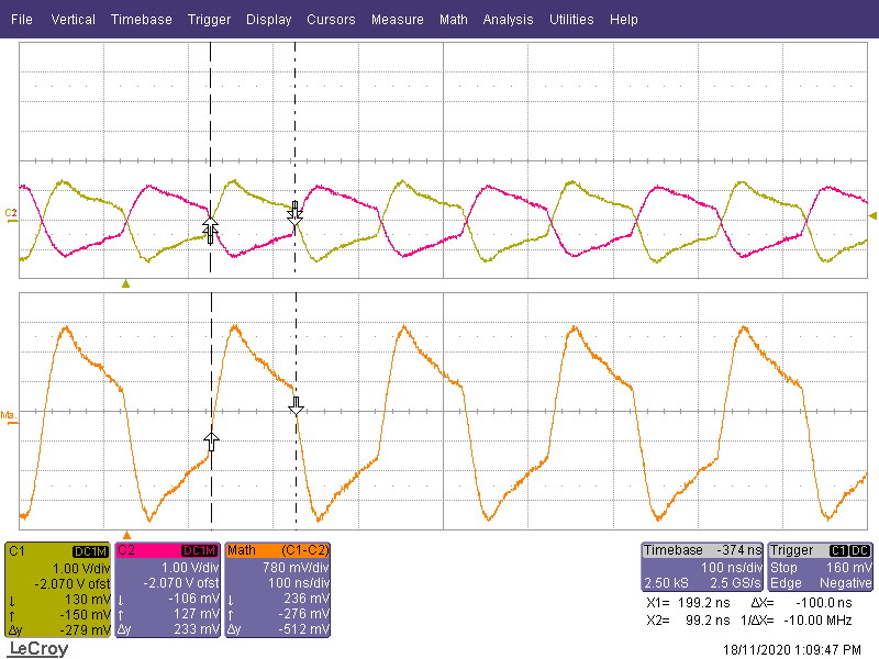
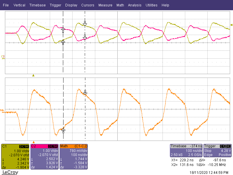
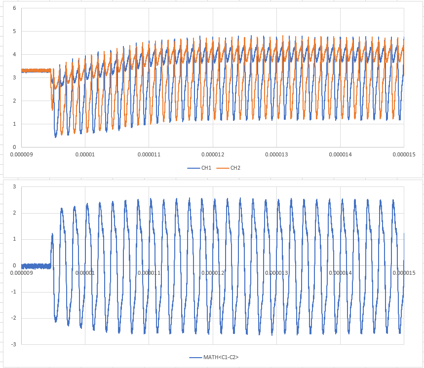
I have done my best to tease some additional information out of LWIP on where I might be going wrong without much success, and have not done anything on the hardware side of things beyond switching out and testing different cables. I haven't bothered probing the signals as I am not sure what I would be looking for anyway.

If anybody has recommendations on where I should be poking around in software or hardware to try and diagnose the issue I would be very thankful.

I have included the relevant section of schematic for our mainboard, as well as the schematic for the injector board.

  • Hi,

      I'm not sure if I'm able to offer much help here as I don't know what causes your board to sometimes not connect. If your software runs fine on the LauchPad without any connection problem then I don't think it is a software issue. I tend to think it may have something to do with your custom board but I'm unable to say anything that is obvious. The TM4C129 system design guideline doesn't offer any recommendation for PoE design. However, there is a TI reference design that employs PoE. Please find below link. I will suggest you compare the the schematic of the two on the magnetic connections.

    https://www.ti.com/tool/TIDM-TM4C129POE

  • I have just added some jumpers so I was able to power the board separately without POE and plug a cable directly between our board and the other device without the intermediate injection board and I am still seeing the same results.

    On our board I am using TPD4E1B06 as ESD protection on the PHY side instead of as per the solution on the Launchpad, this is listed as an acceptable solution though in www.ti.com/.../spma056.pdf

    I also found slua454 which seems to show a similar topology used for a mid-span POE board.

    www.ti.com/.../slua454.pdf

  • I have done more testing playing with LWIP options (forcing 10Mbs, and turning off MDIX) with no apparent change.

    I then swapped back to using the launchpad which is working perfectly, even when plugged through the POE injector board.

    This leaves me with no other choice but to believe it is some issue in either my PCB layout, jack selection or ESD protection.

    My board layout is below, I think I have followed the recommendations, the only thing I can think of is that the jack is running back over the traces (my application is space constrained and I don't have any room outside the board outline.

  • Hi Hugh,

    Have you put a scope probe on Tx/Rx signals to verify quality? There have been many posted cases of RJ45 jacks builtin magnetics cause issues, likely some kind of impedance mismatch is my best guess. Then surrounding capacitance values or PCB layout can lead to even further signal degradation.  

    I have seen what you describe (slow/no link) with launch pad EVM. Issue was related to the HW link detection register via HAL and SW. Seemingly the link register behavior was intermittent but very correctable by SW. 

    Avoid a sudden jump to execute IP stack assignment until link has been verified.

    //*****************************************************************************
    bool bHaveLink = false;	
    
    bHaveLink = MAP_EMACPHYRead(EMAC0_BASE, 0, EPHY_BMSR)
    		   & EPHY_BMSR_LINKSTAT;
    
    
    while(!bHaveLink)
    {
    	/* Check local network switch link exists */
    	bHaveLink = MAP_EMACPHYRead(EMAC0_BASE, 0, EPHY_BMSR)
    					   & EPHY_BMSR_LINKSTAT;
    }

  • Hi Hugh,

      Thanks for the update. How many custom boards do you have? Is your connection issue only happening to one board or all the boards? 

      The traces under the RJ45 could play a role in your issue. But from my side, it is very difficult to say yes or no with a definitive answer. Unless you can modify the board to prove one way or the other. Can you go through the design guideline again? As can be seen there are no traces under the RJ45 shown in the design guideline.


  • Thanks, I will give the software change a go when I get into the office, just to confirm since I am using lwip, this check would go in the handler where the example code checks if the link has recieved an IP address before beginning communications?

    I have tried 3 boards with similar results.

    In terms of my layout vs the guidelines I have applied them as best as I could interpret for the jack with integrated magnetics, I used saturn PCB to get the trace sizing worked out for my stack up. I am least sure about the ground plane and spacing between the jack and micro.

    From what I understood of the ground plane for the jack I was just meant to keep the plane away from the pins see the small keepout in my previous screenshot, as for the spacing, they are pretty close and it's hard to tell what bits of the design guide to follow as some bits seem to contradict, for example in words it indicates discreet magnetics should be no more than 2.54mm from the jack, and yet the example layout is Mabey 5mm because of the ESD protection.

  • No Problem,

    Hugh Powell said:
    this check would go in the handler where the example code checks if the link has recieved an IP address before beginning communications?

    Place code snip prior to static IP assignment or calling DHCP handler where often passing a bool switch in the call determines the address assignment method.

    Your trace layout looks acceptable though next time perhaps try to keep differential pairs the same length, adding zigzags to the shorter pair works best. My custom PCB was two sided and roughly 4 via existed in each pair but the trace length was kept the same. Non the less it makes a DCHP assignment in milliseconds. BTW did you assign a MAC address to the USER registers? That can easily be overlooked and cause some really strange things to happen.

  • I have had a look now that I have the code in front of me and cant find the best place to insert the check, it looks as though I will need to insert it somewhere inside the LWIP library as the lwIPInit Function that I call both enables the peripheral and assigns the static IP. I tried modifying the library to insert the command between where the hardware is initialized and when the IP settings are applied without too much success.

    I have also removed FB1,FB2,FB3,FB4,C24,C25,C26 from my board to completely remove any possibility of interference from the POE injection side of things. This doesn't seem to have affected anything.

    I have had a probe of the Ethernet signals but would require a more experienced eye to look over them, to give myself the best chance of finding something with the scope we have (only 200MHz bandwidth and no differential probes) I have used forced 10Mbs mode and recorded both the Launchpad and our board to be able to compare.

    To me they don't look to dissimilar however I don't really know what I am looking at not having probed Ethernet signals before. I was surprised to see such a large difference between the TD & RD Pairs but it appears on both the launchpad where things work as well as on our custom board so I am guessing it is just the TM4C PHY.

    I should add to further isolate things the below data is captured while running the enet_lwip example on both boards, running the example see the same symptoms as running my code, slow link establishment, but if connects seems to stay connected.

    In the below plots the + signal is in yellow and - in red.

    Launchpad TD Pair Network Side


    Launchpad TD Pair PHY Side


    Custom Board TD Pair at PHY Side
    (Accidentally at a different time scale to the rest of these plots sorry)


    Launchpad RD Pair At Network Side


    L
    aunchpad RD Pair At PHY Side


    Custom Board RD Pair At PHY Side


    Hopefully some aspect of this is able to allow somebody to point me in the correct direction.

  • And sorry, I should have clarified, I have set the Mac address, and as per the lwip examples check that one has been set before initialising lwip.

  • Hi Hugh,

      Thanks for uploading the scope cap. However, I don't have the knowledge to really decipher based on the scope caps to determine what caused the slow link issue.  The chip on the launchPad as well as the chip on your custom board use the same PHY. Therefore, I don't think the slow link or no link is due to the on-chip PHY. 

      I wonder how many custom boards do you experience with the slow link issue? Can you replicate on all the custom boards you have?

      What if you do a ABA test? Swap the chip from your custom board to the LaunchPad and swap the chip on the LaunchPad to the custom board? If the good chip also experiences the slow or no link issue on your custom board then it is the custom board that you want to focus on, not the on-chip PHY. 

  • I have been able to replicate the issue on all of my boards although this is a pretty low volume device so I have only assembled 3 so far.

    I have actually already done the test of replacing the chip on my custom board (but not swapping it to the launchpad) as I was starting to think that it was taking more and more resets before a link was established, swapping the chip for a new one seems to make it more likely to establish a link than before but I expect this may degrade over time again.

    If I was to spin a new board revision would you have any recommendations I could do to try and avoid this issue on the next revision.

  • Hugh Powell said:
    I tried modifying the library to insert the command between where the hardware is initialized and when the IP settings are applied without too much success.

    Typically check link state prior to making an IP connection to the network. If not mistaken lwiplib.c service timers function checks link state prior to DHCP binding or auto IP for the connection. The one thing that stands out is C1 voltage on custom RD seems to go well above 3.9v, scope shows 4.246v seems a bit excessive. Perhaps check datasheet for maximum differential voltages. Do captures assume probe ground was on the negative side of the differential pair?

        //
        // Service the link timer.
        //
    #if LWIP_AUTOIP || LWIP_DHCP
     if((g_ui32LocalTimer - g_ui32LinkTimer) >= LINK_TMR_INTERVAL)
     {
         g_ui32LinkTimer = g_ui32LocalTimer;
         lwIPLinkDetect();
      }

    void
    lwIPHostTimerHandler(void)
    {
     ~~~ Some code
    
        }
        else if(g_sEnet.eState == iEthNoConnection)
        {
            // Once link is detected start DHCP and wait for a response.
            //
            if(lwIPLocalIPAddrGet() != 0xffffffff)// No IP found
            {
               /* Attempt to assign an IP address via DHCP or
            	* just use the provided Static IP address*/
                EthClientDHCPConnect();
    
                g_sEnet.eState = iEthDHCPWait;
            }
        }


  • My scope capture was done with the probe grounds attached to my system 0v plane and then one probe on + and one on -, I did it this way as we don't currently have a differential probe. In some fortuitous timing we are actually about to get a loaner 4 channel portable scope (with isolated channels) with a higher bandwidth as part of a trial. In terms of probing the circuit without disturbing the signal (noting the trace layout requirements) would you have any recommendations on where and how I should attach the scope to do this test.

    Currently out of the office and will have a dig through the library when I get back but when using a static IP does one need to handle the checks any differently.

  • As per recommendation I have swapped the chip off one of my boards to the launchpad, and the launchpad chip to the board. And now the launchpad has the issue of being slow to obtain the link, although it is getting the link more reliably than on my own board. Likewise the custom board, is back to establishing a link in 2-3 seconds.

    Potentially this shows that something on our custom board is damaging the internal PHY.

    I did try recapturing some more data after this on what the TD pair is doing on the custom board (measured between the magnetics and TM4C) and I still have the higher than expected voltages.

    I got a capture that represents the start of a packet where we can see both lines start at 3.3V, as well as in the middle of the packet and it looks like the average voltage is slowly rising through the packet.

    If it is real that the voltages are reaching these levels and not just some kind of probing artifact, I guess it would make sense that it is damaging the chip, I cant see anything specific to the ethernet pins but all the IO pins are rated to 3.3V, and I believe have 0.3V ESD protection diodes. On reflection I don't really see that the ESD protection (TPD4E1B06) recommended by TI in the design guide (spma056) would actually be doing anything as its limit is way higher than what is built in, with current starting to flow above 7V. I note that in one of TI's POE designs(TIDUBR9) they use the same ESD protection (SLVU2.8-4) as used on the launchpad, except they have it inserted between the PHY and magnetics, not between the magnetics and connector as on the launchpad, this part doesn't limit voltage with respect to GND but will limit start limiting the differential at 4V.

  • Hi Hugh,

      Thanks for running these tests. I don't know if it is worthwhile if you have a spare new chip that you can put on the custom board. I will expect it to behave normally and gradually degrade. Is this that you saw with your custom boards where the link issue becomes more apparent as time goes. 

      A couple of questions and comments:

      1. According to the datasheet the VTPTD_100 is a nominal 1V and max of 1.05V. Your capture does seem too high. If I read it right, it is approaching 2V on the + signal. 

      2. Can you explain what are the connections for pin 7,6,2,1 in your schematic? I believe below is the schematic for your RJ45.

    3. Looking at the choice of your RJ45 connector, it is without EMI finger. I don't really know what it is implying. Just wanted to bring it up for brainstorming. Is it more susceptible to EMI? I don't really know.  

      4. Your PCB board might have followed the recommendation, Just wanted to know if it is the case as I don't really have a good idea on what caused your slow/no link issue.

      5. Can you clarify how are you connecting the RBIAS pin? Do you have a 4.87kohm (1% precision) pulldown resistor on this pin?

  • 1) To give my scope the best chance of probing the high speed signals I have been using 10BASE-T for these tests as the issue still occurs even at these lower speeds. I believe 10BASE-T has a higher voltage swing

    2) I am using these pins for POE and transmitting two digital signals, similar to the below example I found, to isolate things though I am have disconnected the center taps and am powering my board directly.

    3) I believe the EMI fingers are just little metal tabs that contact the side of the plug when you plug it in so that if you have one of the fancy Ethernet cables with metal in on the sides of the plug they end up connected to the shell of the Ethernet socket.

    4) I am not 100% sure on how to apply some of those as they seem more focused on when using discrete magnetics, on reading through I don't think I have connected the chassis of the plug per the recommendation. I might try to bodge something up to test with a different connection of the metal shell of the plug. I do note though that in most consumer devices, e.g. desktop pcs/laptops etc, 0V is tied to the case which by extension is connected to the shell of the RJ45 connector.

    5) Yep, I have a 4.87k resistor direct to my ground-plane, and I have verified that the correct resistor actually made it onto my board.

  • Hugh Powell said:
    2) I am using these pins for POE and transmitting two digital signals, similar to the below example I found, to isolate things though I am have disconnected the center taps and am powering my board directly.

    Hi Hugh,

    Hey does the AUX power connect to +24v on either side? If so that could be why the differential pair are rising above safe MAX level if the magnetics on custom PCB are not specifically designed for a PPOE powered Ethernet connection. D6 on your first post schematic shows +24v, is that your custom PCB or the injector, assuming that is the injector? 

    Just for kickers what do the PHY voltages look like when custom PCB Ethernet is connect to launch pad via cross over cable without AUX +24v, if it was powered. BTW bravo for getting the LQFP128 package lifted off the launch pad without destroying pads, large ground plane under MCU really makes removal difficult.

  • The design intent was that I am using the two data pairs for transmitting 24V power from the injector board to my custom board, you can see this is brought out through the rectifier D6 in my schematic, the connector J6 usually is just hooked up to some buttons, however I have been using it while debugging to supply power to the board, and connecting the Ethernet direct to our Ethernet switch (instead of via the injection board).

    I think I am within the rating of the magnetics, my board draws <100 mA and the magnetics are rated to 350mA

    I will try and dig out a crossover cable and give it a go, noting that my launchpad now has a bad chip on it.

    Changing the chip over wasnt too hard with a cheap hot air station, key worry was melting all the plastic parts around on our board, but kapton tape worked pretty well to protect stuff.

  • I did some more probing today with a new scope we have on loan as a trial, unfortunately I messed up some of the data recording not being 100% used to the interface for saving data.

    What I did manage to capture a broad view of was a complete packet (in 10BASE-T) mode.

    Key things I notice is that the two lines seem to drift up by 0.8V over the first 2us or so, notably the differential voltage doesn't change much but I would have expected the peak voltages of 5V are beyond what the pins on the micro can deal with.

  •  Hi Hugh,

      I wonder if the slow or no link connection is due to the "walking-wounded" PHY or missing pulses during the handshake phase between the MCU and the link partner. I myself is also new to the physical layer protocol. So I'm learning as I'm speaking. I found the below articles that talks about auto-negotiation in details. Basically, I'd like to know if the pulses are generated and acknowledged from the protocol standpoint. If all the pulses are generated correctly and received during negotiation and there is still slow or no link then I think the MCU PHY is probably in a walking-wounded state where it sometimes work and sometimes not. 

      I also have a few more questions.

      - Can you confirm if you enable auto-negotiation? If you use the default lwipopts.h then the auto-neg is enabled as in:

    #define EMAC_PHY_CONFIG (EMAC_PHY_TYPE_INTERNAL | EMAC_PHY_INT_MDIX_EN | \
    EMAC_PHY_AN_100B_T_FULL_DUPLEX)

      - Can you confirm if you run the TivaWare examples such as enet_lwip, you will still see the slow/no link issue. The reason I'm asking is because the example will enable the PHY in auto-negotiation mode. However, in your earlier reply and the scope cap, you seem to suggest you force into 10-BASE-T. Correct me if I'm wrong. 

      - Do you remember if your custom boards start out ok but gradually degrade with slow or no link over time? Or immediately the custom board start out with slow or no link connection?

      - Do you have any spare new chips that you can try on the custom board? What I want to know if they will start out ok but gradually degrade over time.

    www.iol.unh.edu/.../Clause_28_Auto-Negotiation.pdf

    http://www.ethermanage.com/ethernet/pdf/dell-auto-neg.pdf

    www.iol.unh.edu/.../Copper_ANEG_JEFF_LAPAK.pdf

  • I think the boards start ok and get worse over time, for example the launchpad chip I put on the custom board works fine art the moment.

    I  see the same behaviour with auto negotiation, that's what I had originally I have only forces 10 Mbit white testing now.

    I am currently all out of chips except for the one I transferred of the launchpad..

    I have tried some of the other examples and see the same behaviour.

  • ok, the chip seems to degrade over time. I found this below post that has very similar issue as yours. Please take a look. Your chip is likely in a walking-wounded state. In the below post, the issue was attributed to the missing ESD. I understand you have ESD in your design. 

    https://e2e.ti.com/support/microcontrollers/other/f/908/t/739571

    See if you can capture the NLP if you are in 10BASE-T mode or FLP if you are in auto-negotiation mode. 

  • Another question is - are you placing the TPD4E1B06 protection diode as close as possible to the connector?

  • Hi Hugh,

    J6 +24 and D6 +24 share a common trace? Feeding J6 dc supply +5vdc when connected to network versus +24v? Perhaps 10k pull downs on the PHY side of MCU would keep the voltage from floating upward,maybe try 3v Zener diodes. Any differential input voltage greater than that listed in datasheet is sure to damage PHY. I think you stated the ESD protection clamps >4v so it will not stop floating voltages.  

    Your posted schematic is confusing since the lower half shows J1 goes to custom board side. Yet you answered custom PCB is powered via J6 +24v, is normally some switches. The J4 is marked industrial controller side and that makes it seem custom PCB has two RJ45's jacks. You did not answer if the top of the schematic is the injector board or part of the custom PCB.

    Secondly there is no cable connection shown between the two jacks of posted schematic. Are we to assume both RJ's are connected via twisted pair are on the same PCB? It appears that +24v is also on the primary center tap custom PCB (J3->U1->J1->J4) and that seems very odd. The top part of schematic looks like a Simplex connection but the bottom half seems questionable that +24v DC path is any where near the PHY side, marked industrial controller side. 

  • Going through the various questions.

    Charles Tsai said:

    See if you can capture the NLP if you are in 10BASE-T mode or FLP if you are in auto-negotiation mode. 

    I believe this is the NLP Pulse we are seeing measured at the PHY with no cable plugged in.

    Charles Tsai said:

    Another question is - are you placing the TPD4E1B06 protection diode as close as possible to the connector?

    See below board layout, the ESD protection is D5, just above the socket. I have my suspicions that this is a suitable ESD protection component, even though it is listed as acceptable in the TM4C1294 app note the datasheet seems to indicate it will clamp to about 7V with respect to ground.

    Gl said:

    J6 +24 and D6 +24 share a common trace? Feeding J6 dc supply +5vdc when connected to network versus +24v? 

    Yes both are common to each other, what I was trying to convey is that I am just powering the board directly from 24V with the power over Ethernet disconnected. The 24V is dropped down to 5V via a DC-DC module, and then dropped to 3.3V via a linear regulator.

    Gl said:

    Secondly there is no cable connection shown between the two jacks of posted schematic. Are we to assume both RJ's are connected via twisted pair are on the same PCB? It appears that +24v is also on the primary center tap custom PCB (J3->U1->J1->J4) and that seems very odd. The top part of schematic looks like a Simplex connection but the bottom half seems questionable that +24v DC path is any where near the PHY side, marked industrial controller side. 

    The intended ethernet connections are as follows Industrial controller <===> J4 On Adapter Board --- J1 On Adapter Board <===> J5 On Custom Board --- TM4C1294. In my original post the custom board with the TM4C is the upper schematic and the lower schematic is the injection board. Either way the latter set of testing I have been doing is just Industrial controller <===> J5 On Custom Board --- TM4C1294, but now that we have narrowed it down to the device being damaged by unknown causes I don't know if it gets damaged in this configuration or not.

    See the below very simplified sketch showing the magnetics pathways.

  • I find a POE TI reference design that also uses the SLVU2.8-4 ESD diodes. Here is the link to the reference design. https://www.ti.com/tool/TIDM-TM4C129POEAUDIO

    While I don't know if the choice of your ESD diodes is the sole reason for the issue, I just wanted to compare the two diodes from their electrical characteristic point of view. The clamping voltage on the TPD4E (10.9-14.5V) is higher than the SLVU2.8 (4-5.5V) for the same test condition. 

    TPD4E:

    SLVU2.8:

  • Hi Charles, I had already noticed that, I had some detail earlier in this thread, my confusion was the TI design guide that I used when I designed the board indicated the TPD4E1B06 was an acceptable alternative, if this is not the case it is a bit frustrating, but in the interests of moving on with this project it would be good if somebody at TI could confirm if the part is suitable or not so that I can get going with a different board revision. Perhaps something like the ESDS304 would be more appropriate?, noting its low clamping voltage, and it is clamping with respect to ground (which is probably preferable for clamping on the PHY side?

    spma056 said:

    A second solution that can be placed on the device side of the transformer between the termination resistors on the differential pairs and the transformer is TI's TPD4E1B06. This device is not shown in Figure 29.

    Hugh Powell said:

    On reflection I don't really see that the ESD protection (TPD4E1B06) recommended by TI in the design guide (spma056) would actually be doing anything as its limit is way higher than what is built in, with current starting to flow above 7V. I note that in one of TI's POE designs(TIDUBR9) they use the same ESD protection (SLVU2.8-4) as used on the launchpad, except they have it inserted between the PHY and magnetics, not between the magnetics and connector as on the launchpad, this part doesn't limit voltage with respect to GND but will limit start limiting the differential at 4V.

    In addition, what should I be looking at to check if a jack with integrated magnetics is suitable, for example, I am potentially looking at changing to a vertical jack instead of a 90 degree jack to allow me to not run traces under the jack. I found v895-1001-aw which I am interested in using but cant find any guidelines on how I can check if it is appropriate.

  • Hi Hugh,

    Hugh Powell said:
    I had some detail earlier in this thread, my confusion was the TI design guide that I used when I designed the board indicated the TPD4E1B06 was an acceptable alternative, if this is not the case it is a bit frustrating, but in the interests of moving on with this project it would be good if somebody at TI could confirm if the part is suitable or not so that I can get going with a different board revision. Perhaps something like the ESDS304 would be more appropriate?, noting its low clamping voltage, and it is clamping with respect to ground (which is probably preferable for clamping on the PHY side?

    I have posted this question to the Interface forum https://e2e.ti.com/support/interface/f/138/t/959129 so the experts there can provide better guidance. Personally, I will use the SLVU2.8-4 since it is proven in multiple TI designs. You can track and follow up if you have additional questions over there.

    Hugh Powell said:
    In addition, what should I be looking at to check if a jack with integrated magnetics is suitable, for example, I am potentially looking at changing to a vertical jack instead of a 90 degree jack to allow me to not run traces under the jack. I found v895-1001-aw which I am interested in using but cant find any guidelines on how I can check if it is appropriate.

    Sorry, I really can't make recommendation on this as I don't have the knowledge of the pros and cons of each selection. The TI reference design for POE uses the below RJ45 connector. 


    Wanted to give you a heads-up as well. I will be on vacation for the rest of the week as a US holiday coming. There will be delay in my response. 

  • Hi Charles

    I will follow up with the other thread and see what happens.

    That jack is unfortunately not suitable for us as we need to only rectify one of the pairs. I will try and compare specs with that jack with integrated magnetics though.

    Have a good holiday, I hear thanksgiving is a big one over there, will anybody else from TI be responding to forum posts, or is more or less everyone on leave. 

  • Hi Hugh,

      Thank you for the good wishes. The holiday is both Thu and Fri but I myself is taking tomorrow off too. Hopefully, there will be someone in the Interface forum to answer your question. 

  • Hi Hugh,

    Curious what is your 3v3 measuring or VDD to TM4C1294? I ask this as the NLP peak amplitude also seems very high. Perhaps try +12v power supply in lieu of +24v just to see if differential pair voltage changes. BTW if the LDO regulator ground pin is not well wetted odd VDD levels may occur. I had the exact thing occur last year, pressing a bamboo stick on top SMP revealed this issue. When I removed the LDO it became very clear the HAL lead free solder  top of pad had somehow oxidized. 

  • I got the below traces while measuring my 3.3V rail, it looks pretty clean.

    The the below plots, yellow = TX+, green=TX-, Blue=TX+ - TX-, Orange = 3.3V rail

    It also stays very stable while the comms is going on and the peaks voltage rises.

    When I was measuring the link pulses with no cable connected I did manage to capture something strange going on that I didn't understand, where both TX lines track together and spike down then up

    Close up of downwards pulse

    Close up of upwards pulse

    I would appreciate it if anybody has a launchpad or board with the same chip lying around if they could record what their link pulse & comms looks like in order to be able to compare directly.

  • Hi Hugh,

    Hugh Powell said:
    I would appreciate it if anybody has a launchpad or board with the same chip lying around if they could record what their link pulse & comms looks like in order to be able to compare directly.

    There are many examples of Ethernet signal captures posted in this forum. Please add to your Tm4c1294 search string, the word (magnetics). Clock works captures seems very different.

    TM4C1294KCPDT: Ethernet Link Issue - Other microcontrollers forum - Other microcontrollers - TI E2E support forums 

  • I hope you guys had a good thanksgiving up there.

    I did have a search around the forums but wasn't really able to find any traces that showed the actual PHY signals, they all seem to just show a differential signal in the middle of a packet, noting that the blue differential signal in my traces doesnt look to bad if you cant see that it is floating up to a higher common mode voltage than it should be.

    Before I get a new board revision made up, do you think there would be much value in me soldering in an ESDS314 dead bug style as ESD protection with magnet wire or would you expect adding the small leads of the signal lines (say 10mm) would impact the signal too much. If did this I could try and setup some tests to power cycle the board or plug things in and out a large number of times and see if my performance degrades.

  • Hi Hugh,

      Honestly, I have yet to really know if the problem is due to the choice of the TVS diodes or just the non-optimized PCB layout for ESD protection. Can you please go through this app note on how to best design a PCB for ESD protection. I think it will help. 

    https://www.ti.com/lit/an/slva680/slva680.pdf

     Regarding your scope shots, my comment is that they are taken during normal operation (e.g. without ESD event). We don't really have the history on what happened and if it ever happened on an ESD event and how the signals look like. 

  • Hugh Powell said:
    noting that the blue differential signal in my traces doesnt look to bad if you cant see that it is floating up to a higher common mode voltage than it should be.

    Seemingly that float is just the problem and likely due to an impedance mismatch of the RJ45 magnetics relative to the PHY differential pair. Why not try to reduce the magnitude my replacing the magnetics with another closer match? Many posts exist of various RJ45 with internal magnetics others have found to be compatible. Perhaps Charles can assist with that effort, if it were me I'd source another RJ45 well before designing another expensive PCB.

    I notice the magnitude of your differential pair (math) is ±50mV greater than it should be relative to Clock Works captures.

  • Ok, so I think I am finally making some progress on this.

    I got some more chips in to sacrifice and have done a large set of testing to try and identify what exactly it is that is causing the chip to fail.

    I have done a few hundred cycles of the following tests.

    • Keep board powered via lab supply (Without POE), connect and disconnect the Ethernet connection.
      • Worked reliably
    • Keep Ethernet connection (Without POE), power cycle the board.
      • Worked Reliably
    • Connect and disconnect board when being powered via POE
      • Started failing to connect after approx 70 cycles.

    From this I started poking around probing the PHY lines while connecting the Ethernet cable. The below plot is yellow TD+, Green TD-, Orange RD+, Blue RD-

    I am seeing a large spike on one line, usually accompanied by a smaller negative spike on a different line. It seems to vary around, but the spike generally appears to occur on either TD-, RD- or both.

    My theory is that when the cable is being plugged in, one side of a pair gets made first, causing a momentary unbalanced current in the magnetics and the resulting large spikes are not being adequately controlled by the ESD protection.

    When I purchased more sacrificial chips I also got in a few ESDS314 and SLVU2.8-4TR chips to trial.

    I have soldered each of these up dead bug onto my board to try out, and found the following.

    • ESDS314
      • Peak voltages reduced from approx 10V to 7V
    • SLVU2.8-4TR
      • Peak Voltages reduced from approx 10V to 5.5V

    The below plot shows an example of plugging in with the SLVU2.8-4TR installed. (Ignore the blue trace it is hooked up to a current probe around one of the pairs but is much to slow for this timescale (rated 100kHz bandwidth), I might try and measure the current via a small shunt tomorrow.

    I am about to do some more cycle testing with the SLV2.8-4TR to see if this solution is progress.

    I was also thinking it may be worth reducing the filter caps (currently 10uF) on my 24V rail, and introducing some series resistance to try and limit the inrush current which I am guessing is what is causing such a violent spike.

    What I would like some additional advice on is in terms of these spikes what voltage goes one need to try and get to to prevent damage, reading the datasheet indicates that voltages must be kept between VDD-0.3, VCC+0.3 but I note that advertised clamping voltages for the ESDS314 start at 5V and work their way up from there.

  • Hi Hugh,

      Glad that you are making progress on this. Since the SLVU2.8-4 is shown as the recommended TVS in the datasheet and the system design guideline, I will suggest this part to be used. In additional, please also reference the best ESD practices for PCB board design that I sent last time. 

    https://www.ti.com/lit/an/slva680/slva680.pdf


  • Hi Hugh,

    That +5v voltage spike present prior to VDD being raised? Typically any external voltage to the MCU should not be present until VDD reaches a threshold, perhaps +2v9 would be safe. The PHY differential pairs should not have any external power applied to them until VDD threshold is achieved. Charles may have a better explanation as why that may be damaging the PHY.

    Perhaps two series placed reed relays could be safe inline solution to delay supply back feed into the MCU.