This thread has been locked.

If you have a related question, please click the "Ask a related question" button in the top right corner. The newly created question will be automatically linked to this question.

TM4C129ENCPDT: uDMA and GPIO

Part Number: TM4C129ENCPDT


Hello everyone,

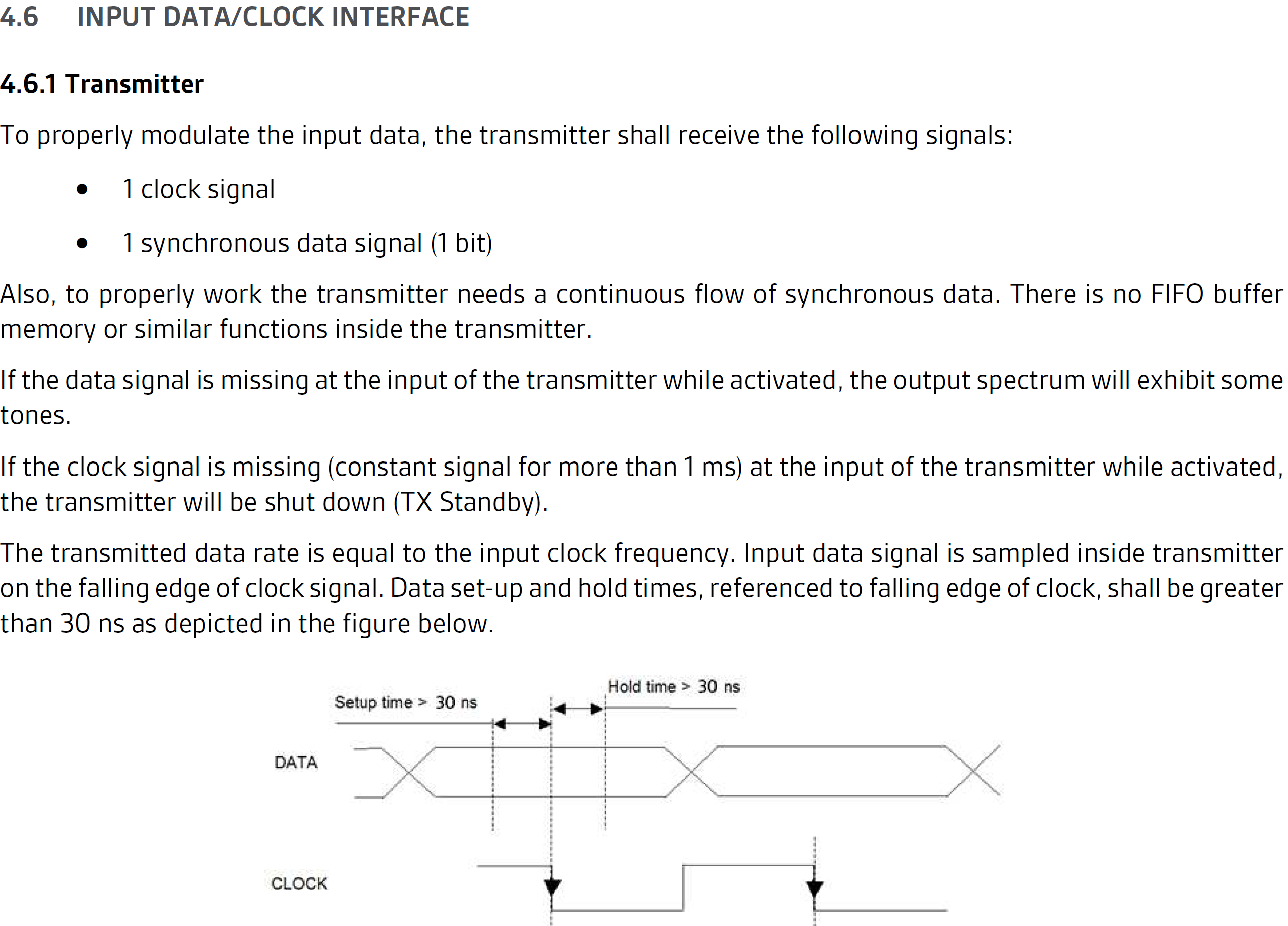
I'm working on developing firmware for TM4C129ENCPDT device. This application is to shift data received from ethernet port then send it to 4 GPIO port A, D, K, L then serial shift them to a radio at 8Mbps. The reason I have to do this is because the radio requires serial RS-422 data input with a synchronous clock which will latch data on falling edge of every bit of serial data. For the serial shift, I used 4 of SN74HC166D (parallel in serial out shift register) so the total serial bit to shift is 32 bit. I plan to use uDMA of the TM4C129 to send data from the ethernet received buffer to GPIO then to load into shift registers, once all 32 bit have been shift out, an external interrupt signal will be generated from shift registers to an input port (port Q) to trigger another transfer until all data is shifted out. I looked around to find examples in Tiva library and didn't find anything similar.

I've studied the uDMA section in the datasheet of the MCU and still unclear about the uDMA channel assignment. From the Table 9-1 page 688 of the datasheet, if I'd like to assign the uDMA channel to GPIO port A, D, K, L then channel 4, 7, 12, and 13 should be used with these functions as below, provided that MCU and these channels have been initialized

MAP_uDMAChannelAssign(UDMA_CH4_GPIOA);
MAP_uDMAChannelAssign(UDMA_CH7_GPIOD);
MAP_uDMAChannelAssign(UDMA_CH12_GPIOK);
MAP_uDMAChannelAssign(UDMA_CH13_GPIOL);

and 

uDMAChannelControlSet(UDMA_CH4_GPIOA | UDMA_PRI_SELECT,
							UDMA_SIZE_8 | UDMA_SRC_INC_32 | UDMA_DST_INC_NONE |
							UDMA_ARB_1);
uDMAChannelControlSet(UDMA_CH7_GPIOD | UDMA_PRI_SELECT,
							UDMA_SIZE_8 | UDMA_SRC_INC_32 | UDMA_DST_INC_NONE |
							UDMA_ARB_1);
uDMAChannelControlSet(UDMA_CH12_GPIOK | UDMA_PRI_SELECT,
							UDMA_SIZE_8 | UDMA_SRC_INC_32 | UDMA_DST_INC_NONE |
							UDMA_ARB_1);
uDMAChannelControlSet(UDMA_CH13_GPIOL | UDMA_PRI_SELECT,
							UDMA_SIZE_8 | UDMA_SRC_INC_32 | UDMA_DST_INC_NONE |
							UDMA_ARB_1);

and 

uDMAChannelTransferSet(UDMA_CH4_GPIOA | UDMA_PRI_SELECT,
			UDMA_MODE_BASIC,
			g_ui8RxBuf, (void *)(GPIO_PORTA_BASE + 0x3FC),
			1);
uDMAChannelTransferSet(UDMA_CH7_GPIOD | UDMA_PRI_SELECT,
			UDMA_MODE_BASIC,
			g_ui8RxBuf, (void *)(GPIO_PORTD_BASE + 0x3FC),
			1);
uDMAChannelTransferSet(UDMA_CH12_GPIOK | UDMA_PRI_SELECT,
			UDMA_MODE_BASIC,
			g_ui8RxBuf, (void *)(GPIO_PORTK_BASE + 0x3FC),
			1);
uDMAChannelTransferSet(UDMA_CH13_GPIOL | UDMA_PRI_SELECT,
			UDMA_MODE_BASIC,
			g_ui8RxBuf, (void *)(GPIO_PORTL_BASE + 0x3FC),
			1);

Please shed some light on this and tell me if I'm in the right direction. Any inputs/comments will be greatly appreciated. Thank you all and have a nice day.

Best Regards,

TLN

  • Interesting application. Why are you not using the SSI to do the serial output? It is much easier to use the uDMA to write to the SSI FIFO than writing to four GPIO ports. Which device is generating the 8MHz clock and the SH/LD- signal, the radio or the TM4C? 

    If the clock and the SH/LD signal come from the radio, and therefore you must use the  SN74HC166D, then have the interrupt routine from the SH/LD rising edge copy the new data to the four GPIO ports. If you need to use uDMA, use a software initiated scatter-gather. The GPIO ports do not initiate the uDMA transfer. The scatter-gather transfers may not be any faster than just doing CPU transfers in the interrupt routine, but it will offload some CPU cycles at the cost of a much more complex initialization

  •  Hello Bob,

    I didn't try to use SSI because my former colleague did a test and he said there was a gap between each byte during the data transfer from received buffer to the radio using SSI (I have not tested myself yet). One characteristic of the radio is if there is a gap between the data and clock signal for a certain time, the radio will stop the transmission. Anyhow, I'll add the data path and utilize the SSI function as you suggested on my schematic and PCB in case I need it as PCB layout is still going on. 

    Controlling the SH/LD signal is done by MCU, the clock signal to shift registers, the interrupt signal when 32 bits are shifted out are generated from CPLD. 

    At first, I was thinking of using an interrupt routine to detect falling edge of signal when 32 bit have been shifted out, but afraid it might take too much MCU resource because receiving data from ethernet port is critical to this application, but I'll try it again when my PCB is built.

    I tested data transfer from buffer to GPIO, I used launchpad board + shift registers on bread board + CPLD development kit, I saw a lot of noise and glitch on the signal, perhaps this due to the bread board and wires I used. Then I try to switch to using uDMA.

    Now I'm leaning on using the uDMA to free up the CPU resource and dedicate it to handle the ethernet data transfer. The idea was when the ethernet receive buffer is filled at a certain level, firmware will initiate the uDMA to transfer data to the shift registers. Once 32 bit have been shifted out, CPLD will generate a external interrupt to port Q of MCU to trigger another uDMA transfer. To test this idea out, I'm searching this forum to see if anyone has done it before and if it's possible to do with TM4C129 MCU, or someone may shed some light or guide me to the right directions.

    Thank you for your response Bob and hope to hear more from this community.

    Best Regards,

    TLN

    PS: The attached is the timing requirement of the data and clock signal to the radio

  • Hello TLN,

    Your image didn't seem to attach correctly.

    TheLam Nguyen said:
    didn't try to use SSI because my former colleague did a test and he said there was a gap between each byte during the data transfer from received buffer to the radio using SSI (I have not tested myself yet). One characteristic of the radio is if there is a gap between the data and clock signal for a certain time, the radio will stop the transmission.

    How many bytes do you need to transfer without a gap? Depending on the amount, it may be possible with TM4C129x as there is a way to use advanced mode to transfer multiple bytes without a gap.

  • Hello Ralph,

    The amount of data to shift out is around 300MB and it must be done in a short time windows. Now I remember the other reason why I didn't want to use SSI was the data format. the data to shift out into the radio must be the LSB first whereas the SSI is MSB first.

    Anyhow I'll study the SSI module in the datasheet and see if there any chances of using it in my application.

    Thank you for your response Ralph. I'll try to attach the image again here.

    Best Regards,

    TLN

  • Changing the bit order does make it more complicated. It still may be possible. The SSI FIFO is 8 entries deep. You can generate an interrupt every time it becomes half empty. At 8M baud, you send one byte every uS. The SSI could generate an interrupt every 4uS. Then you would need to bit reverse and transfer 4 more bytes. (The transfer could easily be done by uDMA, but the bit reversal will require the CPU.) The bit reversal could be very fast using a lookup table like this:

    static const unsigned char TableBitReverse[] = 
    {
      0x00, 0x80, 0x40, 0xC0, 0x20, 0xA0, 0x60, 0xE0, 0x10, 0x90, 0x50, 0xD0, 0x30, 0xB0, 0x70, 0xF0, 
      0x08, 0x88, 0x48, 0xC8, 0x28, 0xA8, 0x68, 0xE8, 0x18, 0x98, 0x58, 0xD8, 0x38, 0xB8, 0x78, 0xF8, 
      0x04, 0x84, 0x44, 0xC4, 0x24, 0xA4, 0x64, 0xE4, 0x14, 0x94, 0x54, 0xD4, 0x34, 0xB4, 0x74, 0xF4, 
      0x0C, 0x8C, 0x4C, 0xCC, 0x2C, 0xAC, 0x6C, 0xEC, 0x1C, 0x9C, 0x5C, 0xDC, 0x3C, 0xBC, 0x7C, 0xFC, 
      0x02, 0x82, 0x42, 0xC2, 0x22, 0xA2, 0x62, 0xE2, 0x12, 0x92, 0x52, 0xD2, 0x32, 0xB2, 0x72, 0xF2, 
      0x0A, 0x8A, 0x4A, 0xCA, 0x2A, 0xAA, 0x6A, 0xEA, 0x1A, 0x9A, 0x5A, 0xDA, 0x3A, 0xBA, 0x7A, 0xFA,
      0x06, 0x86, 0x46, 0xC6, 0x26, 0xA6, 0x66, 0xE6, 0x16, 0x96, 0x56, 0xD6, 0x36, 0xB6, 0x76, 0xF6, 
      0x0E, 0x8E, 0x4E, 0xCE, 0x2E, 0xAE, 0x6E, 0xEE, 0x1E, 0x9E, 0x5E, 0xDE, 0x3E, 0xBE, 0x7E, 0xFE,
      0x01, 0x81, 0x41, 0xC1, 0x21, 0xA1, 0x61, 0xE1, 0x11, 0x91, 0x51, 0xD1, 0x31, 0xB1, 0x71, 0xF1,
      0x09, 0x89, 0x49, 0xC9, 0x29, 0xA9, 0x69, 0xE9, 0x19, 0x99, 0x59, 0xD9, 0x39, 0xB9, 0x79, 0xF9, 
      0x05, 0x85, 0x45, 0xC5, 0x25, 0xA5, 0x65, 0xE5, 0x15, 0x95, 0x55, 0xD5, 0x35, 0xB5, 0x75, 0xF5,
      0x0D, 0x8D, 0x4D, 0xCD, 0x2D, 0xAD, 0x6D, 0xED, 0x1D, 0x9D, 0x5D, 0xDD, 0x3D, 0xBD, 0x7D, 0xFD,
      0x03, 0x83, 0x43, 0xC3, 0x23, 0xA3, 0x63, 0xE3, 0x13, 0x93, 0x53, 0xD3, 0x33, 0xB3, 0x73, 0xF3, 
      0x0B, 0x8B, 0x4B, 0xCB, 0x2B, 0xAB, 0x6B, 0xEB, 0x1B, 0x9B, 0x5B, 0xDB, 0x3B, 0xBB, 0x7B, 0xFB,
      0x07, 0x87, 0x47, 0xC7, 0x27, 0xA7, 0x67, 0xE7, 0x17, 0x97, 0x57, 0xD7, 0x37, 0xB7, 0x77, 0xF7, 
      0x0F, 0x8F, 0x4F, 0xCF, 0x2F, 0xAF, 0x6F, 0xEF, 0x1F, 0x9F, 0x5F, 0xDF, 0x3F, 0xBF, 0x7F, 0xFF
    };

    With the use of multilevel interrupts you might be able to do this while running the ethernet port. Let me see if I can estimate the CPU load.

  • Now back to your original plan. Using the shift registers and the CPLD, you would configure the input from port Q, the SH/LD- signal as your uDMA request. Then you would use a gather-scatter uDMA operation to grab the next four values from the buffer and store then into the four port data registers. I will see if I can find a gather-scatter example that might demonstrate this.

  • Hello Bob,

    I have never used uDMA before and gather-scatter seems to be complicated. I would lean to do it with basic mode first. If I'm not able to use uDMA, then I'll go back to the normal way of writing data to GPIO with CPU involve. The first batch of data to be shifted out is base on the level of received buffer or some other mechanism, thereafter, it's external trigger events. The reason I have to make it to 32 bit of shift register is to account the time to send data out to the GPIO ports in the worse case scenario. At 8Mbps, each bit takes 125ns, with 32 bit I have total 4ms to handle the interrupt and data loading to GPIO. With MCU running at 120MHz, each instruction will take 8.33ps. I need to figure out how many clock cycles MCU needs to do all of the task above to transfer data to the GPIO.

    With the use of uDMA, I believe the CPU will have more time to handle other task on ethernet connection.

    The bit reversal and a LUT seems to be a good alternative approach to this problem, but I need to modify the schematic to accommodate this option.

    Thank you very much for your inputs. Hope to hear back from you and community more.

    Best Regards,

    TLN

  • I can help you with setting up the uDMA, but first let's determine in SSI is a possibility or not. By using advanced mode, we can send a continuous clock as shown in the first image below.

    I am working from home so I only have a USB logic analyzer. The clock periods are all the same, but the logic analyzer resolution makes some of them look uneven when I try to capture a long string.

    There is a complication. Running at 120MHz system clock, the SSI is clocked at half that rate or 60MHz. 8MHz is not an even divisor of 60MHz. Therefore the actual baud rate I got was closer to 8.6M baud (60MHz / 7). To get more exactly 8M baud I need to run the system clock at 112Hz. How close to 8M baud must the data rate be? If 8.6M baud is good enough, I will proceed to calculate the CPU overhead with the bit reversal. If not, I will look into how to set the PLL to 112MHz.

        SSIConfigSetExpClk(SSI0_BASE, ui32SysClock, SSI_FRF_MOTO_MODE_0,
                           SSI_MODE_MASTER, 8000000, 8);
        SSIAdvModeSet(SSI0_BASE, SSI_ADV_MODE_WRITE);
        SSIAdvFrameHoldEnable(SSI0_BASE);
        //
        // Enable the SSI0 module.
        //
        SSIEnable(SSI0_BASE);
    

  • I went ahead and measured the interrupt overhead time using the CPU to load the SSI register. My initial run used an embarrassing 40% of the CPU time. Then I replaced the TivaWare calls with direct register writes in the interrupt routine and got the interrupt time down to 7.2%. I am measuring an I/O pin (GPIO PA3) to determine the interrupt time. The time measured includes one write to the GPIO pin register, but does not include the entry and exit to the interrupt routine.

    The interrupt routine looks like this:

    void SSI0_intRoutine(void)
    {
        unsigned int i;
    
    //  GPIOPinWrite(GPIO_PORTA_BASE, GPIO_PIN_3, GPIO_PIN_3); // pin high
        HWREG(0x40058000 + (GPIO_PIN_3 << 2)) = GPIO_PIN_3;
        // stuff 4 more characters in the SSI FIFO
        for(i = 0; i < 4; i++)
        {
    //      SSIDataPutNonBlocking(SSI0_BASE, TableBitReverse[pui8DataTx[index++]]);
            HWREG(SSI0_BASE + 8) = TableBitReverse[pui8DataTx[index++]];
        }
        if(index >= NUM_SSI_DATA)
        {
            index = 0;
        }
    //  GPIOPinWrite(GPIO_PORTA_BASE, GPIO_PIN_3, 0); // pin low
        HWREG(0x40058000 + (GPIO_PIN_3 << 2)) = 0;
    }
    

    I have exported by CCSv10 project into a .zip file and attached it for your reference.

    /cfs-file/__key/communityserver-discussions-components-files/908/SPI_5F00_Bit_2D00_reverse.zip

  • I realized that we can come closer to 8M baud by using the 16MHz PIOSC (precision internal oscillator) as the SSI clock source. The specified accuracy with the factory calibration is shown in the table below:

    To do the recalibration, your design must have the 32.768-kHz external crystal. My board using only factory calibration at room temperature showed very close to 8MHz baud rate:

    The modified project is attached:

    /cfs-file/__key/communityserver-discussions-components-files/908/7713.SPI_5F00_Bit_2D00_reverse.zip

  • Hello Bob,

    I'm so sorry for being late to respond to your messages because I machine took some updates and froze for a long period of time.

    I'll study your code and try to understand how you've done it. What hardware are you using to achieve this may I ask? Currently I'm waiting on the PCB layout to be completed then get the board built. I hope I can understand your approach and incorporate it to my design to have another option. I truly appreciate your help and guidance. It'll take me some time to study it, and for sure I'll come back with questions. Once again, thank you very much, and have a wonderful day sir.

    Best Regards,

    TLN 


  • No problem. I did my work on the EK-TM4C1294XL launchpad. Don't hesitate to follow up with any questions. 

    You have probably seen this, but wanted to be sure you are aware of this document:

    https://www.ti.com/lit/an/spma056/spma056.pdf

  • Hello Bob,

    Yes, the document is one of guidelines I used for my design. Thank you sir!

    Best Regards,

    TLN

  • Hello Bob,

    I really like the way you do bit reversal using LUT, it's very clever and efficient. Thank you sir!

    Best Regards,

    TLN

  • Hello Bob,

    I study your code and have few dump questions. When you use the function:

    IntRegister(INT_SSI0, SSI0_intRoutine);
    • Don't we still need to register function SSI0_intRountine in the startup_ccs.c file to map it into the interrupt vector table?
    • The Initial routine initialize PA3 for interrupt as an output, but in the interrupt routine you toggle it. Perhaps you use it to signal the end of data transmission. Could you please explain it a bit more?

    Thank you for your help, and for sure I'll come back with more questions.

    Best Regards,

    TLN

  • TheLam Nguyen said:

    I study your code and have few dump questions. When you use the function:

    1
    IntRegister(INT_SSI0, SSI0_intRoutine);
    • Don't we still need to register function SSI0_intRountine in the startup_ccs.c file to map it into the interrupt vector table?

    No, there are two methods of setting the interrupt vectors. You need to do only one of them. Modifying startup_ccs.c modifies the vector table stored in flash and is the most "efficient" in terms of memory usage and code execution. Using the IntRegister() function copies the flash table to RAM and then adds the new vector. It is the more flexible method as you can dynamically change interrupt routines (though this is hardly ever done). I chose to use the IntRegister() function simply because it made the change more visible as it is in main.c instead of startup_ccs.c.

    TheLam Nguyen said:
    The Initial routine initialize PA3 for interrupt as an output, but in the interrupt routine you toggle it. Perhaps you use it to signal the end of data transmission. Could you please explain it a bit more?

    I use PA3 only as a digital output pin. It is simply used to indicate what time is spent in the interrupt routine. I included the trace of this pin on the logic analyzer pictures. In the final product, this would most likely be removed.

  • Hello Bob,

    Roger that. I've added the needed hardware and change my schematic to have SSI option onto my board. I'll test it out when the board is done. When I have the test results, I'll let you know. Thank you very much and appreciate for your help and guidance, have a wonderful day sir.

    Best Regards,

    TLN