This thread has been locked.

If you have a related question, please click the "Ask a related question" button in the top right corner. The newly created question will be automatically linked to this question.

EK-TM4C1294XL: I2C slave ACK

Part Number: EK-TM4C1294XL
Other Parts Discussed in Thread: PCF8574A

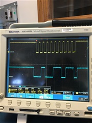
I added 10 K pullup resistors to the I2C lines. Yesterday, the CLK and data lines were clearly visible from the scope. The eval board I used yesterday blew up and I brought in a new one today. I hooked it up and I am running the I2C loopback example (no slave connected, UART printf commented out) and the I2C clock won't show up on the scope. The pullups still measure 10 K. The eval board is OK, it runs blinky. I am out of ideas.

Thanks,

Priya

CLK came back. I made some multimeter measurements

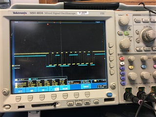
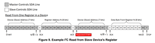
The clock issue is resolved. However, I need to understand how the slave ACK works. The part is pcf8574a, an 8 bit I2C I/O expander chip with no registers. If I write the address and wait, I don't see any I2C CLK trigger on the scope. I2C activity is visible only when after I2CMasterControl(I2C0_BASE, I2C_MASTER_CMD_SINGLE_SEND);

Do you have any pointers on what to do about the ACK signal?

Thanks 

Priya

uint32_t g_ui32SysClock;
int main(void)
{
volatile uint32_t ui32Loop;

//
// The I2C0 peripheral must be enabled before use.
//
SysCtlPeripheralEnable(SYSCTL_PERIPH_I2C0);

//
// For this example I2C0 is used with PortB[3:2]. The actual port and
// pins used may be different on your part, consult the data sheet for
// more information. GPIO port B needs to be enabled so these pins can
// be used.
// TODO: change this to whichever GPIO port you are using.
//
SysCtlPeripheralEnable(SYSCTL_PERIPH_GPIOB);

//
// Configure the pin muxing for I2C0 functions on port B2 and B3.
// This step is not necessary if your part does not support pin muxing.
// TODO: change this to select the port/pin you are using.
//
GPIOPinConfigure(GPIO_PB2_I2C0SCL);
GPIOPinConfigure(GPIO_PB3_I2C0SDA);

//
// Select the I2C function for these pins. This function will also
// configure the GPIO pins pins for I2C operation, setting them to
// open-drain operation with weak pull-ups. Consult the data sheet
// to see which functions are allocated per pin.
// TODO: change this to select the port/pin you are using.
//
GPIOPinTypeI2CSCL(GPIO_PORTB_BASE, GPIO_PIN_2);
GPIOPinTypeI2C(GPIO_PORTB_BASE, GPIO_PIN_3);

g_ui32SysClock = SysCtlClockFreqSet((SYSCTL_XTAL_25MHZ |
SYSCTL_OSC_MAIN |
SYSCTL_USE_PLL |
SYSCTL_CFG_VCO_480), 120000000);

//Initialise relevent peripherals and ports

while (!SysCtlPeripheralReady(SYSCTL_PERIPH_GPIOB));


SysCtlPeripheralDisable(SYSCTL_PERIPH_I2C0);
SysCtlPeripheralReset(SYSCTL_PERIPH_I2C0);
SysCtlPeripheralEnable(SYSCTL_PERIPH_I2C0);


// Initialize Master and slave for 400 kbps //extern uint32_t g_ui32SysClock;
I2CMasterInitExpClk(I2C0_BASE, g_ui32SysClock, false); //fast mode = true (400 kb/s)
I2CMasterEnable(I2C0_BASE);

while(1)
{

I2CMasterSlaveAddrSet(I2C0_BASE, MOSFET_ADDRESS, 1);
for(ui32Loop = 0; ui32Loop < 200000; ui32Loop++)
{
}

I2CMasterDataPut(I2C0_BASE, RED);
I2CMasterControl(I2C0_BASE, I2C_MASTER_CMD_SINGLE_SEND);
for(ui32Loop = 0; ui32Loop < 200000; ui32Loop++)
{
}

/*
I2CMasterSlaveAddrSet(I2C0_BASE, MOSFET_ADDRESS, 0);
I2CMasterDataPut(I2C0_BASE, GREEN);
I2CMasterControl(I2C0_BASE, I2C_MASTER_CMD_SINGLE_SEND);
for(ui32Loop = 0; ui32Loop < 200000; ui32Loop++)
{
}
I2CMasterSlaveAddrSet(I2C0_BASE, MOSFET_ADDRESS, 0);
I2CMasterDataPut(I2C0_BASE, AMBER);
I2CMasterControl(I2C0_BASE, I2C_MASTER_CMD_SINGLE_SEND);
for(ui32Loop = 0; ui32Loop < 200000; ui32Loop++)
{
}
*/

}

}

  • Hi Priya,

    CLK came back. I made some multimeter measurements

    Is this issue resolved now?

  • Here is a picture of the I2C write. The data gets written before the ACK comes from the slave.

  • Hello Priya,

    Rather than waiting in the loop you set, use this instead:

        //
        // Wait until the I2C transaction is complete.
        //
        while(MAP_I2CMasterBusy(I2C0_BASE))
        {
        }

    You can reference this example as well [Install Path]\TivaWare_C_Series-2.2.0.295\examples\boards\ek-tm4c1294xl-boostxl-senshub\humidity_sht21_simple

    And our I2C app note: http://www.ti.com/lit/pdf/spma073

  • Ralf,

    I updated the code pasted below. The slave address is 0x26. I see the start condition. There is a total of 9 visible clock cycles in the overlay. Is the last 1 on the SDA line the ACK? I don't see the data byte I am trying to write to this part. I want to make sure I have the Tiva transfer setup correctly. Do I also post this in the interface forum?

    I really appreciate your help.

    Data byte GREEN is 0x02.

    Thanks,

    Priya

    uint32_t g_ui32SysClock;
    int main(void)
    {
    volatile uint32_t ui32Loop;

    //
    // The I2C0 peripheral must be enabled before use.
    //
    SysCtlPeripheralEnable(SYSCTL_PERIPH_I2C0);

    //
    // For this example I2C0 is used with PortB[3:2]. The actual port and
    // pins used may be different on your part, consult the data sheet for
    // more information. GPIO port B needs to be enabled so these pins can
    // be used.
    // TODO: change this to whichever GPIO port you are using.
    //
    SysCtlPeripheralEnable(SYSCTL_PERIPH_GPIOB);

    //
    // Configure the pin muxing for I2C0 functions on port B2 and B3.
    // This step is not necessary if your part does not support pin muxing.
    // TODO: change this to select the port/pin you are using.
    //
    GPIOPinConfigure(GPIO_PB2_I2C0SCL);
    GPIOPinConfigure(GPIO_PB3_I2C0SDA);

    //
    // Select the I2C function for these pins. This function will also
    // configure the GPIO pins pins for I2C operation, setting them to
    // open-drain operation with weak pull-ups. Consult the data sheet
    // to see which functions are allocated per pin.
    // TODO: change this to select the port/pin you are using.
    //
    GPIOPinTypeI2CSCL(GPIO_PORTB_BASE, GPIO_PIN_2);
    GPIOPinTypeI2C(GPIO_PORTB_BASE, GPIO_PIN_3);

    g_ui32SysClock = SysCtlClockFreqSet((SYSCTL_XTAL_25MHZ |
    SYSCTL_OSC_MAIN |
    SYSCTL_USE_PLL |
    SYSCTL_CFG_VCO_480), 120000000);

    //Initialise relevent peripherals and ports

    while (!SysCtlPeripheralReady(SYSCTL_PERIPH_GPIOB));


    SysCtlPeripheralDisable(SYSCTL_PERIPH_I2C0);
    SysCtlPeripheralReset(SYSCTL_PERIPH_I2C0);
    SysCtlPeripheralEnable(SYSCTL_PERIPH_I2C0);


    // Initialize Master and slave for 400 kbps //extern uint32_t g_ui32SysClock;
    I2CMasterInitExpClk(I2C0_BASE, g_ui32SysClock, false); //fast mode = true (400 kb/s)
    I2CMasterEnable(I2C0_BASE);


    while(1)
    {

    I2CMasterSlaveAddrSet(I2C0_BASE, MOSFET_ADDRESS, 0);

    I2CMasterDataPut(I2C0_BASE, GREEN);
    I2CMasterControl(I2C0_BASE, I2C_MASTER_CMD_SINGLE_SEND);
    while(I2CMasterBusy(I2C0_BASE))
    {
    }

    for(ui32Loop = 0; ui32Loop < 200000; ui32Loop++)
    {
    }

    /*
    I2CMasterSlaveAddrSet(I2C0_BASE, MOSFET_ADDRESS, 0);
    I2CMasterDataPut(I2C0_BASE, GREEN);
    I2CMasterControl(I2C0_BASE, I2C_MASTER_CMD_SINGLE_SEND);
    for(ui32Loop = 0; ui32Loop < 200000; ui32Loop++)
    {
    }
    I2CMasterSlaveAddrSet(I2C0_BASE, MOSFET_ADDRESS, 0);
    I2CMasterDataPut(I2C0_BASE, AMBER);
    I2CMasterControl(I2C0_BASE, I2C_MASTER_CMD_SINGLE_SEND);
    for(ui32Loop = 0; ui32Loop < 200000; ui32Loop++)
    {
    }
    */

    }

    }

  • Hello Priya,

    The waveform doesn't look quite right to me. An ACK would be a low, not a high. See this app note for details: https://www.ti.com/lit/an/slva704/slva704.pdf

    I may not be able to run your code today to test, so I hope the resources I shared help get you moving forward. I am not sure the Interfaces forum would help as I think that is a TM4C issue currently.

  • MosfetI2C.zip

    I am still using TivaWare_C_Series-2.1.4.178

    I have attached the exported project to this message and the scope picture of the single byte transfer out of the I2C as seen on the scope. Of the first 8 CLK cycles visible, the address seen is 01001100. The MOSFET address is 0x26 and the scope is showing 0x4C. Is this the WRITE signal with a 0 shifted into the LSB? I need this confirmed and explained as needed. The attached scope picture seems to show a proper start condition, the address and a NACK.

    Figure 8 of the app note slva704.pdf does not show the start condition. It shows the 8 data bits followed by the ACK.

    Looking forward to your response.

    Priya

  • Hello Priya,

    Is this the WRITE signal with a 0 shifted into the LSB? I need this confirmed and explained as needed.

    Yes. That is how the 7-bit slave address works.

    Figure 8 did show the start condition, maybe you meant Figure 7. But I think Figure 9 makes it a little clearer since the R/W bit toggles.

    On this image, you see the device address write first. It shows the Start Condition, A6 to A0, and then a 0 bit for the R/W bit followed by Ack. So the 0x4C you see is actually 0x26 with a 0 for the write bit. Then you can look at the the third packet where they use a Repeated Start, and this time sending the device address shows A6-A0 and then a 1 bit for R/W to indicate the read followed by the ack.