Other Parts Discussed in Thread: HALCOGEN
Hi,
I am working for data transfer between two TMS570LC4357 controllers, both side MibSPI-1 connected with CS0, CLK, MISO[0], MOSI[0] and ENA pins. I am using the code to configure DMA from example. The data transfer is fine when I have tested with ECOUNT as 4 and FCOUNT as 4. As per my application requirement configured the DMA buffer transfer with ECOUNT as 94 and FCOUNT as 4. The transfer is initially OK, but after few transfers, the data started rolling. I have started checking with the SPI analyzer.
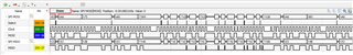
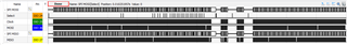
The CS insertion with 4X4 data is much clear and the CS was inserted regularly. With the bigger buffer transfer, the CS looks bit different, and would like to check what could be the possible issue.
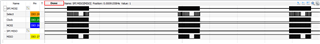
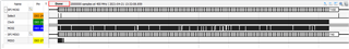
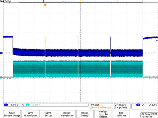
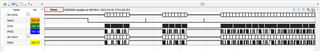
The entire buffer looks like this.
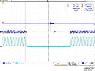
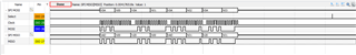
Zoom in the first section (there are 2 first set of identical buffers)
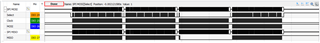
Further zoom (each is of 4 words of 16 bit each)
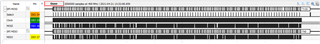
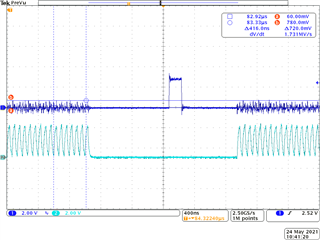
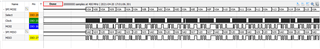
Zoom the large buffer (there are 90 words of 16 bit each)
In total 4+4+90+4+4+90+4+4+90+4+4+90 (total 98 x 4)
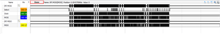
The CS is not uniform during the bigger buffer as below (Not sure why?)
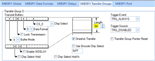
The DMA configuration as below.
/* - initialize transfer groups */
mibspiREG1->TGCTRL[0U] = (uint32)((uint32)1U << 30U) //oneshot
| (uint32)((uint32)0U << 29U) //pcurrent reset
| (uint32)((uint32)TRG_ALWAYS<< 20U) //trigger event
| (uint32)((uint32)TRG_DISABLED << 16U) //trigger source
| (uint32)((uint32)0U << 8U); //start buffer
mibspiREG1->TGCTRL[1U] = (uint32)((uint32)1U << 30U) //oneshot
| (uint32)((uint32)0U << 29U) //pcurrent reset
| (uint32)((uint32)TRG_ALWAYS << 20U) //trigger event
| (uint32)((uint32)TRG_DISABLED << 16U) //trigger source
| (uint32)((uint32)98U << 8U); //start buffer
//MibSPI1 TG0
for (i=0; i<3; i++)
{
mibspiRAM1->tx[i].control = (uint16)((uint16)5U << 13U) //buffer mode
| (uint16)((uint16)1U << 12U) //chip select hold
| (uint16)((uint16)0U << 10U) //enable WDELAY
| (uint16)((uint16)0U << 11U) //lock transmission
| (uint16)((uint16)0U << 8U) //data format
| ((uint16)(~((uint16)0xFFU ^ (uint16)CS_0)) & (uint16)0x00FFU); //chip select
}
mibspiRAM1->tx[3].control = (uint16)((uint16)5U << 13U) //buffer mode
| (uint16)((uint16)0U << 12U) //chip select hold
| (uint16)((uint16)0U << 10U) //enable WDELAY
| (uint16)((uint16)0U << 8U) //data format
| ((uint16)(~((uint16)0xFFU ^ (uint16)CS_0)) & (uint16)0x00FFU); //chip select
//MibSPI1 TG1
for (i=4; i<7; i++)
{
mibspiRAM1->tx[i].control = (uint16)((uint16)5U << 13U) //buffer mode
| (uint16)((uint16)1U << 12U) //chip select hold
| (uint16)((uint16)0U << 10U) //enable WDELAY
| (uint16)((uint16)0U << 11U) //lock transmission
| (uint16)((uint16)0U << 8U) //data format
| ((uint16)(~((uint16)0xFFU ^ (uint16)CS_0)) & (uint16)0x00FFU); //chip select
}
mibspiRAM1->tx[7].control = (uint16)((uint16)5U << 13U) //buffer mode
| (uint16)((uint16)0U << 12U) //chip select hold
| (uint16)((uint16)0U << 10U) //enable WDELAY
| (uint16)((uint16)0U << 8U) //data format
| ((uint16)(~((uint16)0xFFU ^ (uint16)CS_0)) & (uint16)0x00FFU); // chip select
/* TG start address. PSTARTx stores the start address of the corresponding TG. The corresponding */
/* end address is inherently defined by the subsequent TG start address minus 1 (PENDx[TGx] = */
/* PSTARTx[TGx+1]-1). PSTARTx is copied into PCURRENTx when:*/
for(i=0; i<8; i++)
{
tgPSTART1[i] = (mibspiREG1->TGCTRL[i] >> 8) & 0xFF;
}
I have given enough delay for both CS and ENA pins before and after insertion.
The data is also simple array of UINT16 size.
Looking help to understand what could be the issue and how to solve.
Chandra