Hello,
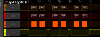
I am communicating with NCV7708 double hex driver via SPI with msp432p401r uC.
According to NCV7708 datasheet when i write to ncv chip i should simultaneously read written data from chip.
But unfortunately what i write doesnot simultaneously comes at MISO. Alternatively it comes at next clock cycles which i send for the next command.
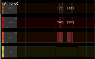
Previously in our old products we have used Atmel XMEGA256A3U uC with ncv chip and there what we write comes simultaneously on MISO as written in ncv datasheet.
Can someone please guide me what i am doing wrong in my code for msp432p401r spi communication.I have attached my code file and spi waveforms.
Many thanks,
#include "msp.h"
#include <stdint.h>
#include <stdlib.h>
#include <stdbool.h>
#include <string.h>

/*! Global Variables defined for debugging */
uint8_t tx_byte_0, tx_byte_1, rx_byte_0,rx_byte_1;
uint16_t rx_16;

/*! Chip Select P5.7 */
#define NCV7708F_BSP_CS_IO_PORT P5
#define NCV7708F_BSP_CS_IO_PIN  BIT7
/*! Chip Enable P3.0 */
#define NCV7708F_BSP_CE_IO_PORT P3
#define NCV7708F_BSP_CE_IO_PIN  BIT0
/*! SPI pins CLK|MOSI|MISO P1.5|P1.6|P1.7| */
#define NCV7708F_BSP_SPI_IO_PORT P1
#define NCV7708F_BSP_SPI_IO_CLK  BIT5
#define NCV7708F_BSP_SPI_IO_MOSI BIT6
#define NCV7708F_BSP_SPI_IO_MISO BIT7

/*! SPI Settings. */
/*! Master | Synchronous | 3Pin SPI | ClockPolarity: inactive at 0 |ClockPhase: 0 | LSB First. */
#define NCV_SPI_Settings EUSCI_B_CTLW0_SWRST | EUSCI_B_CTLW0_MST | EUSCI_B_CTLW0_SYNC
//#define NCV_SPI_Settings EUSCI_B_CTLW0_SWRST | EUSCI_B_CTLW0_MST | EUSCI_B_CTLW0_SYNC | EUSCI_B_CTLW0_CKPH /*! Master | Synchronous | 3Pin SPI | ClockPolarity: inactive at 0 |ClockPhase: 1 | LSB First. */

/*! SMC clock source. */
#define NCV_SPI_CLK EUSCI_B_CTLW0_SSEL__SMCLK

/*! Baud rate = fBRCLK/(UCBRx+1) = 12M/3 = 4 MHz */
#define NCV_SPI_RATE 0x03;

void clk_init(void);
void gpio_init(void);
void spi_init(void);
uint8_t spi_write_and_read_byte(const uint8_t byte);
void write_input_data(const uint16_t value);

int main(void) {

    WDT_A->CTL = WDT_A_CTL_PW | WDT_A_CTL_HOLD; /*! Stop WDT. */

    gpio_init(); /*! Initialize NCV GPIO. */

    clk_init();  /*! Configure Clock 12 MHz. */

    /*! Delay after chip enable. */
    __delay_cycles(96e3); /*! System clock 12e6 so 96e3 = 8 msec. */

    spi_init();  /*! SPI settings. */

    uint16_t value;

    value = 1028;//0000 0100 0000 0100//0x4 0x4;
    write_input_data(value);

    //__delay_cycles(12e3); /*! 1 msec. */

    value = 260; //0000 0001 0000 0100 //0x4 0x1
    write_input_data(value);

    while (1) {
    }

}

void clk_init(void) {

    /*! Configure Clock. */
    /*! SMCLK = MCLK = 12MHz, ACLK = REFOCLK. */
    /*! Unlock CS module for register access*/
    CS->KEY = CS_KEY_VAL;
    /*! Reset tuning parameters. */
    CS->CTL0 = 0;
    /*! Set DCO to 12MHz (nominal, center of 8-16MHz range). */
    CS->CTL0 = CS_CTL0_DCORSEL_3;
    /*! Select ACLK = REFO, SMCLK = MCLK = DCO. */
    CS->CTL1 = CS_CTL1_SELA_2 | CS_CTL1_SELS_3 | CS_CTL1_SELM_3;
    /*! Lock CS module from unintended accesses. */
    CS->KEY = 0;
}


void gpio_init(void) {

    /*! Chip Enable P3.0. */
    NCV7708F_BSP_CE_IO_PORT->DIR |= NCV7708F_BSP_CE_IO_PIN;
    NCV7708F_BSP_CE_IO_PORT->OUT &= ~NCV7708F_BSP_CE_IO_PIN;    /*! Initially Disabled: Low. */

    /*! Chip Select P5.7. */
    NCV7708F_BSP_CS_IO_PORT->DIR |= NCV7708F_BSP_CS_IO_PIN;
    NCV7708F_BSP_CS_IO_PORT->OUT |= NCV7708F_BSP_CS_IO_PIN;     /*! Initially unselected P5.7 High. */

    /*! SPI pins CLK|MOSI|MISO P1.5|P1.6|P1.7| */
    NCV7708F_BSP_SPI_IO_PORT->SEL0 |= NCV7708F_BSP_SPI_IO_CLK | NCV7708F_BSP_SPI_IO_MOSI | NCV7708F_BSP_SPI_IO_MISO;

    /*! Chip Enabled: High.*/
    NCV7708F_BSP_CE_IO_PORT->OUT |= NCV7708F_BSP_CE_IO_PIN;

}


void spi_init(void) {

    /*! Put eUSCI state machine in reset. */
    EUSCI_B0->CTLW0 |= EUSCI_B_CTLW0_SWRST;
    EUSCI_B0->CTLW0 = NCV_SPI_Settings;
    EUSCI_B0->CTLW0 |= NCV_SPI_CLK;
    EUSCI_B0->BRW = NCV_SPI_RATE;
    /*! Initialize USCI state machine. */
    EUSCI_B0->CTLW0 &= ~EUSCI_B_CTLW0_SWRST;

}

uint8_t spi_write_and_read_byte(const uint8_t byte) {

    /*! Wait until USCI_B0 TX buffer is ready. */
    while (!(EUSCI_B0->IFG & EUSCI_B_IFG_TXIFG))
        ;
    /*! Transmit characters. */
    EUSCI_B0->TXBUF = byte;

    /*! Wait till a character is received (this wait is necessary). */
    while (!(EUSCI_B0->IFG & EUSCI_B_IFG_RXIFG))
        ;

    return EUSCI_B0->RXBUF;
}

void write_input_data(const uint16_t value) {

    /*! Select Device. */
    NCV7708F_BSP_CS_IO_PORT->OUT &= (~NCV7708F_BSP_CS_IO_PIN);    /*! P5.7 = low */

    tx_byte_0 = value & 0x00FF;
    tx_byte_1 = (value & 0xFF00) >> 8;

    /*! Send Byte 0. */
    rx_byte_0 = spi_write_and_read_byte(tx_byte_0);

    /*! Send Byte 1. */
    rx_byte_1 = spi_write_and_read_byte(tx_byte_1);

    rx_16  = (uint16_t) (rx_byte_1 << 8) | rx_byte_0;

    /*! Un-select Device. */
    NCV7708F_BSP_CS_IO_PORT->OUT |= (NCV7708F_BSP_CS_IO_PIN);     /*! P5.7 = High */

}