This thread has been locked.

If you have a related question, please click the "Ask a related question" button in the top right corner. The newly created question will be automatically linked to this question.

TMS320F280049C: Tformat encoder experiment :SOMI waveform is abnormal and Clks waveform cannot be captured

Part Number: TMS320F280049C

HI expert,

I use the new code modified from the code that has successfully implemented encoder reading data on F280049C-Launchpad, and the hardware resources are the control board designed by our company (the chip is F280049c).I tried to measure TXen(GPIO5) waveform, SOMI (GPIO10) waveform and Clks (GPIO3) waveform, but unfortunately only TXen waveform looks normal, SOMI looks abnormal, Clks waveform cannot be measured.Their waveforms are shown below:

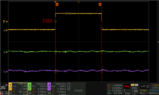
Figure 1: Waveform of TXen

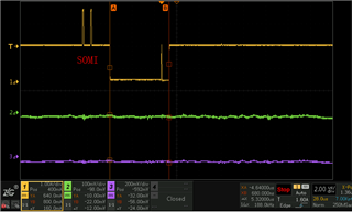
Figure 2: Waveform of SOMI

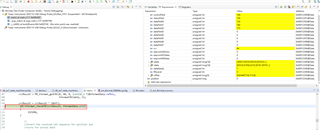
My configuration code is modified as follows: 1.GPIO port;2. XBAR;3.CLB, the specific code is as follows:

void tformat_setupGPIO(void)
{

    //
    // GPIO4 is SPI Clk slave
    //
    GPIO_setMasterCore(4, GPIO_CORE_CPU1);
    GPIO_setPinConfig(GPIO_4_EPWM3A);

    //
    // GPIO8 is the SPISIMOA
    //
    GPIO_setMasterCore(8, GPIO_CORE_CPU1);
    GPIO_setPinConfig(GPIO_8_SPISIMOA);
    GPIO_setQualificationMode(8, GPIO_QUAL_ASYNC);

    //
    // GPIO10 is the SPISOMIA
    //
    GPIO_setMasterCore(10, GPIO_CORE_CPU1);
    GPIO_setPinConfig(GPIO_10_SPISOMIA);
    GPIO_setQualificationMode(10, GPIO_QUAL_ASYNC);

    //
    // GPIO3 is the SPICLKA
    //
    GPIO_setMasterCore(3, GPIO_CORE_CPU1);
    GPIO_setPinConfig(GPIO_3_SPICLKA);
    GPIO_setQualificationMode(3,GPIO_QUAL_ASYNC);

    //
    // GPIO57 is the SPISTEB
    //
    GPIO_setMasterCore(57, GPIO_CORE_CPU1);
    GPIO_setPinConfig(GPIO_57_SPISTEA);
    GPIO_setQualificationMode(57, GPIO_QUAL_ASYNC);


    //
    // GPIO5 is tformat TxEN
    //
    GPIO_setMasterCore(5, GPIO_CORE_CPU1);
    GPIO_setPinConfig(GPIO_5_OUTPUTXBAR3);

}


void tformat_initCLBXBAR() {

    XBAR_setCLBMuxConfig(XBAR_AUXSIG0, XBAR_CLB_MUX01_INPUTXBAR1);
    XBAR_enableCLBMux(XBAR_AUXSIG0, XBAR_MUX01);
    XBAR_setOutputMuxConfig(XBAR_OUTPUT3, XBAR_OUT_MUX09_CLB3_OUT4);
    XBAR_enableOutputMux(XBAR_OUTPUT3, XBAR_MUX09);
}

The questions I would like to ask are as follows:

1.Is my configured correctly? Where are the problems likely to arise?

2.Maybe there is a problem with the hardware, so how should I check?

  • Hi<


    I use the new code modified from the code that has successfully implemented encoder reading data on F280049C-Launchpad, and the hardware resources are the control board designed by our company (the chip is F280049c).

    are you using the same resources when you were experimenting on the F280049C launchpad?

    Did you have to change any GPIO or XBAR configuration from Launchpad to you own hardware?
    Since the hardware is designed by you, I cannot say if the GPIO configuration is correct or not. 
    Make sure the pins/GPIOs are configured according to your h/w.

    Also, check s/w configuration of CLB, SPI before debugging hardware further. Check the clock first and then command going to the encoder.

  • Subrahmanya,

    Thank you very much for your reply.I think the clock signal is generated by CLB, so is my CLB configuration wrong?Where should the clock normally be checked when it is not generated?Hope you can guide, thank you!

    Johnson Alanl

  • Hello,

    I think the clock signal is generated by CLB, so is my CLB configuration wrong?Where should the clock normally be checked when it is not generated?

    Yes, it is generated by the CLB.  I would check the clock in two places (1) the pin where it comes out of the device (i.e. CLB driving) and (2) at the pin where it goes back into the device (i.e. routed back into the SPI).

    Regards

    Lori

  • Lori,

    I am very glad to see your reply and guidance.In fact, my PWM is sent from the PWM3A port and then transmitted to the SPI clock, but I put the oscilloscope probe into the chip PWM3A has no signal, and the SPI clock port has no signal.

    Regards

    Johnson Alanl

  • I put the oscilloscope probe into the chip PWM3A has no signal

    Then check

    • Can you toggle PWM3A using another method?  A simple PWM example or writing to the GPIO registers.  This will check the board connection to the device. 
    • Check the configuration from tile 3 through to the PWM3A   
  • 1.Before, I wondered whether the PWM3A port of the chip was broken. Then I took other examples of TI and burned the program to my development board. I could capture the waveform, which has proved that there should be no problem with the PWM3A port.

    2.Since THE PREVIOUS F280049C-Launchpad used CLB1 (because the clock is output by PWM1B), now I have changed CLB1 to CLB3 (because the clock is output by PWM3A) for my development board, other CLB logic should not need to be changed.

    3.I wonder why IN0 and IN1 are set to sync signal and filter input.Can I change it to another input channel?Such as IN2, IN3...

    CLB_enableSynchronization(CLB3_BASE, CLB_IN0);
    CLB_enableSynchronization(CLB3_BASE, CLB_IN1);

    CLB_selectInputFilter(CLB3_BASE, CLB_IN0, CLB_FILTER_RISING_EDGE);
    CLB_selectInputFilter(CLB3_BASE, CLB_IN1, CLB_FILTER_FALLING_EDGE);

  • 1.Before, I wondered whether the PWM3A port of the chip was broken. Then I took other examples of TI and burned the program to my development board. I could capture the waveform, which has proved that there should be no problem with the PWM3A port.

    Thank you for confirming.

    2.Since THE PREVIOUS F280049C-Launchpad used CLB1 (because the clock is output by PWM1B), now I have changed CLB1 to CLB3 (because the clock is output by PWM3A) for my development board, other CLB logic should not need to be changed.

    Within the CLB the clock output should be moved from CLBx_OUT2 (overrides PWMxB) to CLB_OUT0 (overrides PWMxA).  Refer to the Peripheral Signal Multiplexer Table in the CLB Output Selection section of the Technical Reference Manual (TRM)

    3.I wonder why IN0 and IN1 are set to sync signal and filter input.Can I change it to another input channel?Such as IN2, IN3...

    CLB_enableSynchronization(CLB3_BASE, CLB_IN0);
    CLB_enableSynchronization(CLB3_BASE, CLB_IN1);

    CLB_selectInputFilter(CLB3_BASE, CLB_IN0, CLB_FILTER_RISING_EDGE);
    CLB_selectInputFilter(CLB3_BASE, CLB_IN1, CLB_FILTER_FALLING_EDGE);

    Not sure why you would want to do this - you can, but then the new input assignments would need to be re-routed right logic in the CLB Tile.  

    In the TRM, the CLB input selection describes the synchronizer and the edge filtering. 

  • Thanks for your reply. I'm looking at the TRM.

  • Lori,

    void PM_tformat_startOperation(void)
    {
    EALLOW;
    HWREG(CLB4_BASE + CLB_LOGICCTL + CLB_O_LOAD_EN) |= CLB_LOAD_EN_GLOBAL_EN
    | CLB_LOAD_EN_STOP;

    __asm(" RPT #10 || NOP");
    CLB_setOutputMask(CLB4_BASE, 0x3C, true);
    __asm(" RPT #10 || NOP");
    CLB_setGPREG(CLB4_BASE, 0x81);
    }

    Please help me understand the F28379D example (here using PWMB to output the clock), I think there seems to be a bit of a problem here, because I understand that 0X3C enables OUT2, OUT3, OUT4 and OUT5, but I know by looking at TRM that OUT4 is AQ_PWMA.If I am now the PWMA output clock, should I change 0X3C to 0X13?

  • The internal routing within the CLB will need to change.

    The recommended way to modify the internal CLB configuration is using the CLB tool.  You can find getting started training and documentation described on this post:

    https://e2e.ti.com/support/microcontrollers/c2000-microcontrollers-group/c2000/f/c2000-microcontrollers-forum/1007238/faq-configurable-logic-block-clb---how-do-i-get-started

    For this case, I see two options:

    I see two options

    (1) Move the signal to the desired OUTLUT.  If an equation is also applied to the OUTLUT, take care of that as well.   If something is already allocated to the desired OUTLUT you will need to move it as well and then re-route to an pin.   

    (2) Another option, if available, is to use OUTLUT4 or OUTLUT5 on one one of the tiles - these can be routed to any GPIO via the OUTPUTXBAR.  For example you can rout from Tile y OUTLUT3 --> input on Tile x --> Tile x OUTLUT4 or 5 --> OUTPUTXBAR --> GPIO.

    Regards

    Lori

  • Lori,

    Thank you very much for your guidance. I have something to share with you.

    I used f280049C-Launchpad to test my code and found that I could not capture the CLks waveform either.Later I changed the GPIO port of CLKs from GPIO4(EPWM3A) to GPIO5(EPWM3B) and I was surprised to find that I could measure the correct clock waveform.After my verification and test, it is not GPIO4 that is occupied.And I have also enabled the relevant CLB outlet, may I ask how to solve this problem?

    void PM_tformat_startOperation(void)
    {
        EALLOW;
        HWREG(CLB3_BASE + CLB_LOGICCTL + CLB_O_LOAD_EN) |= CLB_LOAD_EN_GLOBAL_EN
                | CLB_LOAD_EN_STOP;
    
        __asm(" RPT #10 || NOP");
        CLB_setOutputMask(CLB3_BASE, 0xff, true);
        __asm(" RPT #10 || NOP");
        CLB_setGPREG(CLB3_BASE, 0x81);
    }

  • Later I changed the GPIO port of CLKs from GPIO4(EPWM3A) to GPIO5(EPWM3B) and I was surprised to find that I could measure the correct clock waveform

    I believe that the clock is connected to the tile boundary via Tile3 OUTLUT2.  Tile3 OUT2 is connected to the B channel of the PWM (refer to the output selection MUX table 29-3 in the TRM).  So this is expected. 

    To, instead, override the A channel the clock would need to be connected to the tile boundary via Tile 3 OUTLUT0 as shown in the table.  How to approach the move is described in my previous post.

  • Lori,

    Thank you very much for your guidance. My encoder looks like it can read the data, but the code stops at:

    if(!tformat_checkCRC(crcResult, tformatData.crc))
    {
    ESTOP0;
    }

    Can you give me some guidance on how to solve the problem? Thank you very much!

    Best Regards

    Johnson Alanl

  • First check that this is really where it stops.  If optimization is enabled in the compiler options then the source code debug view maybe misleading.  Check the disassembly window to get a better verification of the PC's location or temporarily turn off optimization in the compiler settings.  

    If this is where the code stops, then the CRC received from the encoder does not match what the C28x calculated.  Since you tested this same algorithm on F2837xD, the algorithm should be fine and it is likely an issue with the data not being captured correctly - perhaps noise or power issues? 

  • Another thing you can do is compare the data to your working system - both coming out of the SPI and using a 'scope.