This thread has been locked.

If you have a related question, please click the "Ask a related question" button in the top right corner. The newly created question will be automatically linked to this question.

TMS320F28379D: Reprogramming FLASH for CPU1 and CPU2

Part Number: TMS320F28379D
Other Parts Discussed in Thread: C2000WARE

Hello,

I'm using CPU1 and CPU2 on TMS320F28379D 

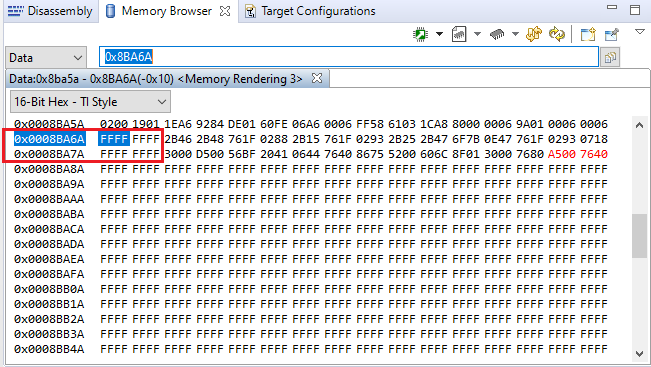
In my software, I want to reprogram FLASH for CPU1 and CPU2 with an HEX file on a SD card (using SPI-A).
For information, on a previous program, I used only CPU1 and this function (FLASH reprogramming with SD card) works fine.

The reprogramming process is as follow : 

  • Read HEX file information's
  • Erase CPU1 Flash sectors
  • Write HEX file data's in FLASH
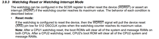
  • Reboot CPU1 with watchdog

Below how I want to proceed : 

  • In normal state, CPU1 program and CPU2 program are synchronized with IPCs flags.
  • If CPU1 reprogramming is in progress; CPU2 is in "idle" state. SPI-A is drived by CPU1.
  • When CPU1 reprogramming is done, CPU1 send an IPC (IPC0) flag to CPU2 to start reprogramming (interrupt on CPU2),change SPI-A ownership (CPU1 -> CPU2) then reboot.
  • CPU2 reprogramming is in progress; CPU1 is in "idle" state. SPI-A is drived by CPU2.
  • When CPU2 reprogramming is done, CPU2 reboot.
  • When both core will reboot, we will be in normal state.

I can reprogram CPU1 FLASH correctly, but I have some questions for CPU2 reprogramming : 

  • During CPU1 Flash programming process, SPI-A is drived by CPU1. I tried to change SPI-A ownership to CPU2 after CPU1 reboot, but it seems it doesn't works. Why ?

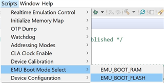
  • After CPU1 programming and reboot, I already have "Illegal_ISR", maybe it's due to the Debug mode on Code Composer after a reboot. How can I debug CPU2 program ?

Regards,

  • Hello, 

    For the CPU1 programming and reboot, where is the beginning of the program? Is it the Flash entry point? Is there a call stack that shows how the illegal ISR is reached? 

    For the SPI question I have requested the SPI expert to comment. 

    Thanks, 

    Anu

  • Hello,

    I tried to change SPI-A ownership to CPU2 after CPU1 reboot, but it seems it doesn't works. Why ?

    Can you please provide the code you are using to change the ownership? 

    Are you modifying the CPUSEL6 register, specifically bit 0 (SPIA)?

    Best Regards,

    Marlyn

  • Hello Marlyn,

    This is the code I used : 

    EALLOW;
    DevCfgRegs.CPUSEL6.bit.SPI_A = 1;           // SPIA controlled by CPU2
    EDIS;

    Can I execute this code just after writing data's in Flash, but before rebooting CPU1 ?
    Because I want SPI-A be driven by CPU2 only after a CPU1 reprogramming ; in normal operation, SPI-A will be drive by CPU1.

    Regards,

  • Anu,

    Yes, it is the Flash entry point.

    In final operation, CPU1 and CPU2 will reboot on FLASH, that's why I use the instruction : 

    IPCBootCPU2(C1C2_BROM_BOOTMODE_BOOT_FROM_FLASH);

    But for debug test, I removed this instruction.

    Is there a call stack that shows how the illegal ISR is reached?

    I don't understand your request, how can I proceed ?

    For me it could be normal to have an issue, as I'm in debug mode, after a reboot, Code Composer will be disconnected, no ?

    Regards,

  • I've made several tests today. I've tried the entire loop, without FLASH operation and reboot : 

    • CPU1 read HEX file informations (on SD card)
    • CPU1 give SPI-A ownership to CPU2, send IPC0 flag to CPU2, then leave SD card reading function. I didn't re-enable interrupts, so CPU1 is in "idle" state, because my software is base on an external interrupt. CPU1 execute Main loop (no functions inside)
    • IPC0 interrupt is triggered on CPU2, so I start SD reading functions.
    • I can read SD card informations with CPU2, which means SPI-A ownership is on CPU2.

    So it works. The issue is when I erase FLASH sectors on CPU1 and CPU2, and when I try to reboot both core.

    • On CPU1 side : 
      • After erasing FLASH sectors and re-writing FLASH with my HEX file, how must I proceed to send IPC0 flag to CPU2 and change SPI-A ownership to CPU2 ?
      • If I reboot CPU1 after writing FLASH, I will restart my software and all my Init functions, so in normal operation, SPI-A is drived by CPU1.
      • So CPU1 must be in "idle state" before rebooting, but how can I proceed ?
    • On CPU2 side : 
      • Same questions, how must I proceed ?

    Thanks for your support.

    Regards,

  • Hello, 

    After erasing FLASH sectors and re-writing FLASH with my HEX file, how must I proceed to send IPC0 flag to CPU2 and change SPI-A ownership to CPU2 ?

    This could be a part of the new hex file you are writing into Flash. The instructions can be placed after your init functions.

    • If I reboot CPU1 after writing FLASH, I will restart my software and all my Init functions, so in normal operation, SPI-A is drived by CPU1.
    • So CPU1 must be in "idle state" before rebooting, but how can I proceed ?

    I am not clear here, what state is CPU1 in if not idle before rebooting? It sounds like that is the case here based on this:

    CPU1 give SPI-A ownership to CPU2, send IPC0 flag to CPU2, then leave SD card reading function. I didn't re-enable interrupts, so CPU1 is in "idle" state, because my software is base on an external interrupt. CPU1 execute Main loop (no functions inside)

    For this: 

    On CPU2 side : 
    • Same questions, how must I proceed ?

    Can the same functionality in the operations of CPU2 before the rewriting not be repeated here? Is Flash properly written to with the new image before CPU2 starts executing here - maybe you are reading from erased Flash?

    Thanks, 

    Anu

  • Hello,

    This could be a part of the new hex file you are writing into Flash. The instructions can be placed after your init functions.

    Yes, but these functions (send IPC flag to CPU2 and change SPI-A ownership to CPU2) must be executed only if we have a reprogramming.
    In normal operation (reboot with no reprogramming), CPU1 must drive SPI-A and doesn't send IPC0 flag to CPU2.

    If we have a reprogramming, after CPU1 reboot : 

    • CPU1 send IPC flag (interrupt) to CPU2
    • CPU1 change SPI-A ownership to CPU2
    • CPU1 "wait" until CPU2 reprogramming is done

    If we have no reprogramming, after a simple reboot : 

    1. CPU1 has SPI-A ownership
    2. CPU1 execute his standard loop.

    To solve this point, I write a value in a part of the FLASH (which is not erased during reprogramming) if I have a reprogramming, but before all the reprogramming process.
    When I reboot CPU, I read this value and I know if there was a reprogramming or not.
    Hope I'm clear on this point.

    The main issue I have is CPU's reboot. As I explained below, when I remove Flash (erase and writing) operations and reboot, the loop between CPU1 and CPU2 is done correctly.

    If I use reboot function in Debug mode, it's normal to have an interrupt on Code Composer ? I've tried to do Flash operations & reboot on CPU1 only, I have this interrupt : 

    //
    // Illegal Operation Trap
    //
    interrupt void ILLEGAL_ISR(void)
    {
        //
        // Insert ISR Code here
        //
    
        //
        // Next two lines for debug only to halt the processor here
        // Remove after inserting ISR Code
        //
        asm ("      ESTOP0");
        for(;;);
    }

    Does my CPU1 reboot function is correct ? 

            EALLOW;
            WdRegs.SCSR.all = 0x0000; // Configuration : Generate a reset signal
            EDIS;
    
            EALLOW;
            WdRegs.WDKEY.all = 0x0055; // Clear the WDCNTR bits
            WdRegs.WDKEY.all = 0x00AA; // Clear the WDCNTR bits
            EDIS;
    
            EALLOW;
            WdRegs.WDCR.all = 0x0028; // Enable the watchdog
            EDIS;
    
            EALLOW;
            WdRegs.WDKEY.all = 0x0055; // Do not clear the WDCNTR bits to generate the reset signal
            WdRegs.WDKEY.all = 0x0000; // Do not clear the WDCNTR bits to generate the reset signal
            EDIS;

    Does the WD reboot only CPU1 or both CPUs ?

    Regards,

  • Hello, 

    I will check on whether rebooting the CPU while in debug mode causes an ITRAP. This link can also help you figure out why the CPU is going into an ITRAP: https://software-dl.ti.com/C2000/docs/c28x_interrupt_faq/html/index.html

    Are you trying to generate a watchdog timeout? It looks like you are following the correct steps. 

    The watchdog reset affects CPU1 and CPU2 as follows: 

    Thanks, 

    Anu

  • Hello Anu,

    Yes, I just want CPU's reboot, that's why I use a watchdog timeout. Is it the correct way to proceed ?

    Ok, so a watchdog reset on CPU1 affects both CPUs.

    So if I want to use debug mode and do online test after a reboot, I need to set the emulation flash boot for both CPUs before running, am I right ? 

    I made a very simple test : 

    • I've loaded software on CPU1 and CPU2
    • Before running, I've set emulation flash boot on EMU_BOOT_FLASH for both CPUs (CPU2 then CPU1).
    • Both program are running.
    • When there's a request, CPU1 just read SD card informations, then reboot.
    • I've put a breakpoint in my init functions for CPU1, to see if CPU1 correctly reboot, but it seems the program never stops here.
    • Then program is not working anymore.

    How can I know where am I in the program ?

    Do I need to use this instruction for CPU1 ?

    CpuSysRegs.RESC.bit.WDRSn = 1;

    Waiting also for your answer concerning the ITRAP.

    Thanks for your support.

    Regards,

  • Hello, 

    Rebooting the CPU while in Debug mode on its own would not be a reason to cause an ITRAP - is the Flash entry point populated with the code_start function? If the contents of the codestartbranch file are not written into the Flash entry point, the CPU may be executing some garbage instructions which could be the reason for the ITRAP to be generated. Can you check the map file of the image that is supposed to run after the reboot and see if the codestartbranch file is mapped to the Flash entry point?

    To generate a watchdog timeout, writing to the SCSR register and the WDCR register should be sufficient. 

    To see where you are in the program, it may also be helpful to see what the contents of the stack are during the ITRAP, the return address should be there. 

    Thanks, 

    Anu

  • Hello Anu,

    As I explained, during my last tests, I don't have ITRAP anymore, but I don't know if my program reboot correctly ; is my procedure (below) correct ?

    I made a very simple test : 

    • I've loaded software on CPU1 and CPU2
    • Before running, I've set emulation flash boot on EMU_BOOT_FLASH for both CPUs (CPU2 then CPU1).
    • Both program are running.
    • When there's a request, CPU1 just read SD card informations, then reboot.
    • I've put a breakpoint in my init functions for CPU1, to see if CPU1 correctly reboot, but it seems the program never stops here.
    • Then program is not working anymore.

    Thanks for your support.

    Regards,

  • I will check with a teammate and get back to you within a couple of days.

    Thanks

    Anu

  • Hello,

    Any update ?

    Regards,

  • Hi,

    Anu is out of office today.  We will review and get back to you early next week.

    Thanks and regards,

    Vamsi

  • Hello,

    Any update ?!

    Regards,

  • Hi,

    Sorry for late reply. 

    • When there's a request, CPU1 just read SD card informations, then reboot.
    • I've put a breakpoint in my init functions for CPU1, to see if CPU1 correctly reboot, but it seems the program never stops here.

    In this case, does CPU1 goes through reset cycle after reading info from SD card ? When you halt the CPU after reboot, what is the PC value ?

    Regards,

    Vivek Singh

  • Ok, I see from your original post that you are using the WD reset to reboot CPU1. You also understand that CPU1 WD reset will reset CPU1 as well as CPU2 both so I hope you have made change in you flow to program CPU1 and CPU2 both and then reboot CPU1 using WD reset which will reboot CPU2 as well. 

    Is that correct ?

    Regards,

    Vivek Singh

  • Hello Vivek,

    Yes, I'm using WD to reset CPU1. It's clear for me that CPU1 WD will reset CPU2 too.

    First thing I want to check is if the WD reboot CPU1 ; this is how I proceed : 

    • In CPU1 software, I put a breakpoint in my init function, before the main loop.
    • I load software on CPU1 and CPU2
    • Before running, I set emulation flash boot on EMU_BOOT_FLASH for both CPUs (CPU2 then CPU1).
    • I run both programs.
    • Program stops on CPU1 init function breakpoint (normal), I restart it.
    • Both program are running.
    • When there's a request, CPU1 just read SD card informations, then reboot, using the WD reset.
    • My program doesn't stop on CPU1 init function breakpoint.

    Do you know why ? I hope I was clear with my explainations.

    It's the first point to solve, after I'll explain as I want to proceed to program both CPU.

    Regards,

  • After WD reset (for reboot), have you checked emulation flash boot  (EMU_BOOT_FLASH) is still set ? When you halt the CPU1 where does it stop (PC value) ? Please check the value in RESC and NMISHDFLG register also after the halt.

    Regards,

    Vivek Singh 

  • Hello Vivek,

    How can I check emulation flash boot after the reset ?

    I will do the test Monday

    Regards,

  • Hi,

    How can I check emulation flash boot after the reset ?

    You put a hardware breakpoint in reset vector (in BOOT ROM) (basically the PC where CPU points after you issue a debug reset) and CPU should halt there after WD reset and then you can check the value. You can also check the new image and see if it was programmed correctly.

    Regards,

    Vivek Singh

  • Hello Vivek,

    When I halt the CPU1, value of registers are : 

    • RESC : 0xC0000004
    • NMISHDFLG : 0x0000

    Programs stops in an interrupt, that means it didn't stops in my breapoint (asm ("      ESTOP0");) after my Init ; dit it really reboot ?

  • You put a hardware breakpoint in reset vector (in BOOT ROM) (basically the PC where CPU points after you issue a debug reset) and CPU should halt there after WD reset and then you can check the value. You can also check the new image and see if it was programmed correctly.

    Sorry, but how proceed to do this ? I never did it before.

    Regards,

  • Programs stops in an interrupt, that means it didn't stops in my breapoint (asm ("      ESTOP0");) after my Init ; dit it really reboot ?

    Did you check the value at address 0xD00 after CPU halts at above point ?

    Regards,

    Vivek Singh

  • Hello Vivek,

    You mean when I halt the CPU ? I'll check tomorrow the value of EMUBOOTCTRL (address 0xD00)

    How can I proceed to put a hardware breakpoint in reset vector ?

    Thanks for your support Vivek.

    Regards,

  • How can I proceed to put a hardware breakpoint in reset vector ?

    As I mentioned earlier, when you reset the CPU, jut put the breakpoint where PC is pointing (open disassembly view and add breakpoint).

    Reagrds,

    Vivek Singh

  • Vivek,

    I'm sorry if I ask questions bit it's not very clear for me.

    If I've understood, I've to reset the CPU a first time, see where PC is pointing (by opening the disassembly view), and add a breakpoint ?
    How can I add a breakpoint in the disassembly view ?
    Then I have to relaunch my program ?

    Thanks for your support, and sorry for these questions.

    Regards,

  • If I've understood, I've to reset the CPU a first time, see where PC is pointing (by opening the disassembly view), and add a breakpoint ?

    Just double click on the line you want to set a breakpoint. 

    Then I have to relaunch my program ?

    You don't have to relaunch the program. Just run it after setting the breakpoint. Program is already loaded in flash so it should work.

    Regards,

    Vivek Singh

  • Hi, 

    Were you able to get it working ?

    Regards,

    Vivek Singh

  • Hello Vivek,

    Sorry, I was in vacation.

    Old issue is solved, CPU1 reboot after a watchdog reset in emulation mode. But the main issue isn't. Just to explain the situation : 

    I want to reprogram CPU1 and CPU2 ; for both CPU's, the goal is to convert the .out file in an HEX file, store this one on a SD card, read it then writing in FLASH the HEX file.

    I have issue with

    2 different cases (I just explain for CPU1): 

    • In emulation mode, I comment this line : 

    //IPCBootCPU2(C1C2_BROM_BOOTMODE_BOOT_FROM_FLASH);

    I build the .out file, convert to .HEX file, copy it on the SD card, read the SD card, write the FLASH correctly. It works.

    • In standalone mode, I add this line : 

    IPCBootCPU2(C1C2_BROM_BOOTMODE_BOOT_FROM_FLASH);

    I build the .out file, convert to .HEX file, copy it on the SD card, read the SD card, write the FLASH ; it doesn't works.
    The .out file, so the .HEX file, is not exactly the same, I'm agree with that.
    In my .HEX file, some lines have changed, and one in particularly.


    The number of bytes of this line has changed, and now I have and issue for writing in FLASH.

    Is it because I use Fapi_AutoEccGeneration in the function Fapi_issueProgrammingCommand() ?

    To program, I follow instructions in chapter 10 : 

    https://e2e.ti.com/support/microcontrollers/c2000-microcontrollers-group/c2000/f/c2000-microcontrollers-forum/951668/faq-faq-on-flash-api-usage-for-c2000-devices

    When I want to program address 0x8BA66, it doesn't works. 

    Do you know why ?

    Thanks for your support.

    Regards

  • Hi,

    Why do you need to comment out IPC boot command code in emulation mode. You should be able to run exact code in emulation mode also and if it fails then debug it. You should be able to reset CPU1/CPU2 and then run CPU1 and then CPU2 and it should work just like standalone.

    Regards,

    Vivek Singh

  • Vivek,

    I follow this procedure : https://e2e.ti.com/support/microcontrollers/c2000-microcontrollers-group/c2000/f/c2000-microcontrollers-forum/735910/ccs-tms320f28377d-cpu2-boot-from-flash

    Now I can be in Emulation mode using a flash mode reboot. You're right I didn't have to comment IPC boot command code.

    But it doesn't solve my issue. I cannot write some datas in FLASH, I don't understand why : 

    Datas write in FLASH (.HEX file) : 

    Datas writted in FLASH after erase & reprogramming : 

    Looks like datas at @0x8BA66 are not writted, but I don't know why.

    Regards,

  • Hi,

    Now that you are able to run the same code with emulator connected, you should be able to step through the code and find the error code when trying to program the flash. I find it strange that you are facing issue with only one specific address. I'll also loop in our flash expert to look into this.

    Regards,

    Vivek Singh

  • Hi,

    In your linker cmd file, do you have all the sections aligned on 128-bit boundary? You can use ALIGN(8) to achieve this.

    Please take a look at the flash based linker cmd files provided in the C2000Ware for the usage of ALIGN().

    Thanks and regards,

    Vamsi 

  • Hello Vamsi,

    Please find in attached my cmd file. I follow your instructions, there's an offset on the address but issue is the same : 

    MEMORY
    {
    PAGE 0 :  /* Program Memory */
              /* Memory (RAM/FLASH) blocks can be moved to PAGE1 for data allocation */
              /* BEGIN is used for the "boot to Flash" bootloader mode   */
    
        BEGIN           	: origin = 0x080000, length = 0x000002
        RAMM0           	: origin = 0x000122, length = 0x0002DE
        RAMD0           	: origin = 0x00B000, length = 0x000800
        RAMLS03          : origin = 0x008000, length = 0x002000
        //RAMLS0          	: origin = 0x008000, length = 0x000800
        //RAMLS1          	: origin = 0x008800, length = 0x000800
        //RAMLS2      		: origin = 0x009000, length = 0x000800
        //RAMLS3      		: origin = 0x009800, length = 0x000800
        RESET           	: origin = 0x3FFFC0, length = 0x000002
       
        /* Flash sectors */
        FLASHABCDEFG       : origin = 0x080002, length = 0x01FFFE		/* on-chip Flash */
        //FLASHA           : origin = 0x080002, length = 0x001FFE		/* on-chip Flash */
        //FLASHB           : origin = 0x082000, length = 0x002000		/* on-chip Flash */
        //FLASHC           : origin = 0x084000, length = 0x002000		/* on-chip Flash */
        //FLASHD           : origin = 0x086000, length = 0x002000		/* on-chip Flash */
        //FLASHE           : origin = 0x088000, length = 0x008000		/* on-chip Flash */
        //FLASHF           : origin = 0x090000, length = 0x008000		/* on-chip Flash */
        //FLASHG           : origin = 0x098000, length = 0x008000		/* on-chip Flash */
        FLASHH           : origin = 0x0A0000, length = 0x008000			/* on-chip Flash */
        //FLASHI           : origin = 0x0A8000, length = 0x008000			/* on-chip Flash */
    
        FLASHK           : origin = 0x0B8000, length = 0x002000			/* on-chip Flash */
        FLASHL           : origin = 0x0BA000, length = 0x002000			/* on-chip Flash */
        FLASHM           : origin = 0x0BC000, length = 0x002000			/* on-chip Flash */
    	FLASHN           : origin = 0x0BE000, length = 0x002000			/* on-chip Flash */
    
    PAGE 1 : /* Data Memory */
             /* Memory (RAM/FLASH) blocks can be moved to PAGE0 for program allocation */
    
        BOOT_RSVD        : origin = 0x000002, length = 0x000120     		/* Part of M0, BOOT rom will use this for stack */
        RAMM1            : origin = 0x000400, length = 0x000400     		/* on-chip RAM block M1 */
        RAMD1            : origin = 0x00B800, length = 0x000800
    
        RAMLS4      		: origin = 0x00A000, length = 0x000800
        RAMLS5      		: origin = 0x00A800, length = 0x000800
    
        RAMGS0      		: origin = 0x00C000, length = 0x001000
        RAMGS1_2_3  		: origin = 0x00D000, length = 0x003000
        RAMGS4_5_6		: origin = 0x010000, length = 0x003000
        //RAMGS5      		: origin = 0x011000, length = 0x001000
        //RAMGS6      		: origin = 0x012000, length = 0x001000
        RAMGS7      		: origin = 0x013000, length = 0x001000
        RAMGS8      		: origin = 0x014000, length = 0x001000
        RAMGS9      		: origin = 0x015000, length = 0x001000
        RAMGS10     		: origin = 0x016000, length = 0x001000
        RAMGS11     		: origin = 0x017000, length = 0x001000
        RAMGS12     		: origin = 0x018000, length = 0x001000
        RAMGS13     		: origin = 0x019000, length = 0x001000
        RAMGS14     		: origin = 0x01A000, length = 0x001000
        RAMGS15     		: origin = 0x01B000, length = 0x001000
    
        CPU2TOCPU1RAM   	: origin = 0x03F800, length = 0x000400
        CPU1TOCPU2RAM   	: origin = 0x03FC00, length = 0x000400
    
    	FLASHI           : origin = 0x0A8000, length = 0x008000			/* on-chip Flash */       // for reboot mode
        FLASHJ           : origin = 0x0B0000, length = 0x008000			/* on-chip Flash */
    
    }
    
    
    SECTIONS
    {
       /* Allocate program areas: */
       //.cinit			: > FLASHABCDEFG		PAGE = 0, ALIGN(4)		/* initialization values for global and static variables */
       //.pinit          	: > FLASHABCDEFG,		PAGE = 0, ALIGN(4)		/* tables for global constructors (C++) */
       //.text        	: > FLASHABCDEFG		PAGE = 0, ALIGN(4)		/* Executable code and constants */
       //codestart       	: > BEGIN				PAGE = 0, ALIGN(4)
       .cinit			: > FLASHABCDEFG		PAGE = 0, ALIGN(8)		/* initialization values for global and static variables */
       .pinit          	: > FLASHABCDEFG,		PAGE = 0, ALIGN(8)		/* tables for global constructors (C++) */
       .text        	: > FLASHABCDEFG		PAGE = 0, ALIGN(8)		/* Executable code and constants */
       codestart       	: > BEGIN				PAGE = 0, ALIGN(8)
    
       /* Allocate uninitalized data sections: */
       //.stack          	: > RAMM1        		PAGE = 1				/* stack space */
       //.ebss         	: >> RAMLS4 |  RAMLS5	PAGE = 1				/* global and static variables */
       //.esysmem        	: > RAMGS0       		PAGE = 1				/* memory for far malloc functions */
       .stack          	: > RAMM1        		PAGE = 1, ALIGN(8)				/* stack space */
       .ebss         	: >> RAMLS4 |  RAMLS5	PAGE = 1, ALIGN(8)				/* global and static variables */
       .esysmem        	: > RAMGS0       		PAGE = 1, ALIGN(8)				/* memory for far malloc functions */
    
       /* Initalized sections go in Flash */
       //.econst        	: >> FLASHABCDEFG		PAGE = 0, ALIGN(4)
       //.switch        	: > FLASHABCDEFG      	PAGE = 0, ALIGN(4)
       .econst        	: >> FLASHABCDEFG		PAGE = 0, ALIGN(8)
       .switch        	: > FLASHABCDEFG      	PAGE = 0, ALIGN(8)
    
       .reset         	: > RESET,     PAGE = 0, TYPE = DSECT 			/* not used, */
    
    #ifdef __TI_COMPILER_VERSION__
        #if __TI_COMPILER_VERSION__ >= 15009000
            GROUP
            {
                .TI.ramfunc
                { -l F021_API_F2837xD.lib}
    
            } LOAD = FLASHABCDEFG,
              RUN  = RAMLS03,
              LOAD_START(_RamfuncsLoadStart),
              LOAD_SIZE(_RamfuncsLoadSize),
              LOAD_END(_RamfuncsLoadEnd),
              RUN_START(_RamfuncsRunStart),
              RUN_SIZE(_RamfuncsRunSize),
              RUN_END(_RamfuncsRunEnd),
              PAGE = 0
        #else
            GROUP
            {
                ramfuncs
                { -l F021_API_F2837xD.lib}
    
            } LOAD = FLASHABCDEFG,
              RUN  = RAMLS03,
              LOAD_START(_RamfuncsLoadStart),
              LOAD_SIZE(_RamfuncsLoadSize),
              LOAD_END(_RamfuncsLoadEnd),
              RUN_START(_RamfuncsRunStart),
              RUN_SIZE(_RamfuncsRunSize),
              RUN_END(_RamfuncsRunEnd),
              PAGE = 0
        #endif
    #endif
    
    
        /* The following section definitions are required when using the IPC API Drivers */
        GROUP : > CPU2TOCPU1RAM, PAGE = 1
        {
            PUTBUFFER
            PUTWRITEIDX
            GETREADIDX
        }
    
        GROUP : > CPU1TOCPU2RAM, PAGE = 1
        {
            GETBUFFER :    TYPE = DSECT
            GETWRITEIDX :  TYPE = DSECT
            PUTREADIDX :   TYPE = DSECT
        }
       
    	//CPU1ExchangeBuffer : > RAMD1			PAGE = 1
       	//CPU1toCPU2Buffer : > CPU1TOCPU2RAM		PAGE = 1
       	//CPU2toCPU1Buffer : > CPU2TOCPU1RAM		PAGE = 1
       	//CalibrationTable : > RAMGS4_5_6			PAGE = 1
    	//SDCard_Memory : > RAMGS7       			PAGE = 1
    	CPU1ExchangeBuffer : > RAMD1			PAGE = 1, ALIGN(8)
       	CPU1toCPU2Buffer : > CPU1TOCPU2RAM		PAGE = 1, ALIGN(8)
       	CPU2toCPU1Buffer : > CPU2TOCPU1RAM		PAGE = 1, ALIGN(8)
       	CalibrationTable : > RAMGS4_5_6			PAGE = 1, ALIGN(8)
    	SDCard_Memory : > RAMGS7       			PAGE = 1, ALIGN(8)
    }
    
    /*
    //===========================================================================
    // End of file.
    //===========================================================================
    */
    

    Thanks for your support.

    Regards,

  • Hi,

    1) As of now, you are loading the hex image to flash using your custom flash programmer - correct?

    2) What happens if you program the hex image using CCS?  Does it cause the same issue?  Please check and let me know.

    Thanks and regards,
    Vamsi

  • Hello ,

    1) Yes, I'm loading the hex flash image using a SD card.

    2) You mean if I load the hex image using CCS ? How proceed to do that ?

    Thanks and regards

  • Hi,

    #2. CCS allows you to load a hex file as well.  Did you face any problem loading it?

    Thanks and regards,

    Vamsi

  • Vamsi,

    No issue when I load the hex file with CCS.

    Data are writted correctly : 

    Thanks for your support.

    Regards,

  • Hi,

    Then I don't think the issue is with the hex file or the flash.

    Thanks and regards,

    Vamsi

  • I'm agree, so where can the error come from ?!

    The goal is to use the SD card to load the HEX file and not CCS, so my issue is not solved.

    Regards,

  • Hi,

    You need to check/debug the loader/programmer from SD card. 

    Thanks and regards,
    Vamsi

  • Vamsi,

    This is exactly what I did on my previous posts. I put some breakpoints at different place to find the issue, but I can't find it.

    It's not an aligned memory issue. Address I find the issue is 0x8BA6A, so as described here : e2e.ti.com/.../faq-faq-on-flash-api-usage-for-c2000-devices

    (iii) if the address is “128-bit aligned address+2”, then a max of six 16-bit words can be programmed at a time.

    I have 16 words to write, so I've written 2 words, then 4 words, then 4, 4 words and 2 words. As explained above, 2 words are not writing, but all the others are : 

    Any idea ?

    Thanks and regards.

  • Hi,

    Thank you for reading through my FAQ.

    If I understand correctly, you are talking about the last 2 words that are not written properly.  

    If you program ECC using Fapi_AutoEccGeneration or Fapi_DataAndEcc modes, anytime you program less than 4 words (aligned 64-bits), you need to ensure that the remaining unprogrammed locations in that 4 words (aligned 64-bits) are not programmed again - program operation will fail even though those locations are 0xFFFF.  Reason: ECC is already programmed for that 64-bits assuming 0xFFFF for the unprovided data within that 64-bits.  Now, when you try to program those erased locations, the new ECC value will collide with the existing ECC value - and program will fail.

    Thanks and regards,
    Vamsi

    Flash FAQs: e2e.ti.com/.../faq-flash-frequently-asked-questions

  • Vamsi,

    Thanks for your explaination, it's clear for me now.

    I'll use Fapi_DataOnly, it's more flexible for my application.

    Regards,

  • Hi,

    Glad it helped.

    Please note:  Irrespective of which programming mode you use (Fapi_DataOnly or Fapi_AutoEccGeneration etc), you should program a given 128-bit aligned memory for not more than 4 times (including ECC writes). 

    Let me know if you have any questions.

    Thanks and regards,
    Vamsi  

  • Hello Vamsi,

    Please note:  Irrespective of which programming mode you use (Fapi_DataOnly or Fapi_AutoEccGeneration etc), you should program a given 128-bit aligned memory for not more than 4 times (including ECC writes). 

    Why that ? I never program 128-bit aligned memory at a time, maximum is 64-bit aligned.

    After a reboot (due to my watchdog reset), program stopped in a NMI interrupt. Is it because I use Fapi_DataOnly instead of Fapi_AutoEccGeneration ?
    I disabled ECC to solve it. Is there a specific place to write this code ?

    Last issue I have, after erasing the FLASH and rewriting it, program stops after the reboot, but I don't know what the issue is : 

    I've checked, all the Flash sectors are well programmed. Is it due to ECC again ? 

    Thanks for your support.

  • Hi,

    Today is a holiday for us.  I will get back to you in a day or two.

    Thanks and regards,

    Vamsi

  • Hi Vamsi,

    I've modified my code to use Fapi_AutoEccGeneration instead of Fapi_DataOnly. I also removed the function which disabled ECC.
    I've put a breakpoint at the end of CPU1 Flash writing function ; Flash sectors seems to be well programmed.

    But when I reboot CPU1 with watchdog reset, I have this message : 

    Can you help please ?

    Does "CpuSysRegs.RESC.bit.WDRSn = 1;" instruction has to be used on CPU1 or CPU2 ?

    Regards,

  • Hi,

    That address in the screen shot is NMI handler in BootROM space (as per the TRM's 4.9.2 Wait Points section).

    Please check NMIFLG/NMISHDFLG registers to know the cause for the NMI and fix it.

    Thanks and regards,

    Vamsi