Part Number: TMS320F28335
I have working for a while about jumping from secondary bootloader to application.
I designed two different project for both. In both, I am using two linker files together. First one is DSP2833x_Headers_nonBIOS.cmd (for peripherals) and STL_F28335.cmd (for memory).
STL_F28335 is a variant of linkers which includes safety library functions.
Later, I allocated only FLASHA sector for my secondary bootloader as in the below linker file. I remained same BEGIN entry points in the linker file so, factory boot will leave control secondary at power-up.
/*
//###########################################################################
//
// FILE:	F28335.cmd
//
// TITLE:	Linker Command File For F28335 Device
//
//###########################################################################
// $TI Release: 2833x/2823x Header Files and Peripheral Examples V133 $
// $Release Date: June 8, 2012 $
//###########################################################################
*/

/* ======================================================
// For Code Composer Studio V2.2 and later
// ---------------------------------------
// In addition to this memory linker command file,
// add the header linker command file directly to the project.
// The header linker command file is required to link the
// peripheral structures to the proper locations within
// the memory map.
//
// The header linker files are found in <base>\DSP2833x_Headers\cmd
//
// For BIOS applications add:      DSP2833x_Headers_BIOS.cmd
// For nonBIOS applications add:   DSP2833x_Headers_nonBIOS.cmd
========================================================= */

/* ======================================================
// For Code Composer Studio prior to V2.2
// --------------------------------------
// 1) Use one of the following -l statements to include the
// header linker command file in the project. The header linker
// file is required to link the peripheral structures to the proper
// locations within the memory map                                    */

/* Uncomment this line to include file only for non-BIOS applications */
/* -l DSP2833x_Headers_nonBIOS.cmd */

/* Uncomment this line to include file only for BIOS applications */
/* -l DSP2833x_Headers_BIOS.cmd */

/* 2) In your project add the path to <base>\DSP2833x_headers\cmd to the
   library search path under project->build options, linker tab,
   library search path (-i).
/*========================================================= */

/* Define the memory block start/length for the F28335
   PAGE 0 will be used to organize program sections
   PAGE 1 will be used to organize data sections

    Notes:
          Memory blocks on F28335 are uniform (ie same
          physical memory) in both PAGE 0 and PAGE 1.
          That is the same memory region should not be
          defined for both PAGE 0 and PAGE 1.
          Doing so will result in corruption of program
          and/or data.

          L0/L1/L2 and L3 memory blocks are mirrored - that is
          they can be accessed in high memory or low memory.
          For simplicity only one instance is used in this
          linker file.

          Contiguous SARAM memory blocks can be combined
          if required to create a larger memory block.
 */


MEMORY
{
PAGE 0:    /* Program Memory */
           /* Memory (RAM/FLASH/OTP) blocks can be moved to PAGE1 for data allocation */

   ZONE0       : origin = 0x004000, length = 0x001000     /* XINTF zone 0 */
   RAML0       : origin = 0x008000, length = 0x001000     /* on-chip RAM block L0 */
   RAML1       : origin = 0x009000, length = 0x001000     /* on-chip RAM block L1 */
   RAML2_1     : origin = 0x00A000, length = 0x000AA8     /* on-chip RAM block L2 */
   PC_TEST_1   : origin = 0x00AAA8, length = 0x000004     /* PC test function 1 */
   RAML2_2     : origin = 0x00AAAC, length = 0x000554     /* on-chip RAM block L2 */
   RAML3       : origin = 0x00B000, length = 0x001000     /* on-chip RAM block L3 */
   ZONE6       : origin = 0x0100000, length = 0x100000    /* XINTF zone 6 */
   ZONE7A      : origin = 0x0200000, length = 0x00FC00    /* XINTF zone 7 - program space */
   FLASHH      : origin = 0x300000, length = 0x007FFE     /* on-chip FLASH */
   APP_BEGIN   : origin = 0x307FFE, length = 0x000002
   FLASHG      : origin = 0x308000, length = 0x008000     /* on-chip FLASH */
   FLASHF_1    : origin = 0x310000, length = 0x005558     /* on-chip FLASH */
   FLASHF_2    : origin = 0x315558, length = 0x002AA8     /* on-chip FLASH */
   FLASHE      : origin = 0x318000, length = 0x008000     /* on-chip FLASH */
   FLASHD      : origin = 0x320000, length = 0x008000     /* on-chip FLASH */
   FLASHC_1    : origin = 0x328000, length = 0x002AAC     /* on-chip FLASH */
   FLASHC_2    : origin = 0x32AAAC, length = 0x005554     /* on-chip FLASH */
   FLASHB      : origin = 0x330000, length = 0x008000     /* on-chip FLASH */
   FLASHA      : origin = 0x338000, length = 0x007E78     /* on-chip FLASH */
   PC_TEST_2   : origin = 0x33FE78, length = 0x000004     /* PC test function 2 */
   PC_TEST_3   : origin = 0x33FE7C, length = 0x000004     /* PC test function 3 */
   CRC_TABLE   : origin = 0x33FE80, length = 0x000100     /* Table to hold 32 golden CRC values */
   CSM_RSVD    : origin = 0x33FF80, length = 0x000076     /* Part of FLASHA.  Program with all 0x0000 when CSM is in use. */
   BL_BEGIN    : origin = 0x33FFF6, length = 0x000002     /* Part of FLASHA.  Used for "boot to Flash" bootloader mode. */
   CSM_PWL     : origin = 0x33FFF8, length = 0x000008     /* Part of FLASHA.  CSM password locations in FLASHA */
   OTP         : origin = 0x380400, length = 0x000400     /* on-chip OTP */
   ADC_CAL     : origin = 0x380080, length = 0x000009     /* ADC_cal function in Reserved memory */

   IQTABLES    : origin = 0x3FE000, length = 0x000b50     /* IQ Math Tables in Boot ROM */
   IQTABLES2   : origin = 0x3FEB50, length = 0x00008c     /* IQ Math Tables in Boot ROM */
   FPUTABLES   : origin = 0x3FEBDC, length = 0x0006A0     /* FPU Tables in Boot ROM */
   ROM         : origin = 0x3FF27C, length = 0x000D44     /* Boot ROM */
   RESET       : origin = 0x3FFFC0, length = 0x000002     /* part of boot ROM  */
   VECTORS     : origin = 0x3FFFC2, length = 0x00003E     /* part of boot ROM  */
   BOOT_RSVD   : origin = 0x000000, length = 0x000050     /* Part of M0, BOOT rom will use this for stack */
   RAMM0       : origin = 0x000050, length = 0x0003B0     /* on-chip RAM block M0 */
   RAMM1       : origin = 0x000400, length = 0x000400     /* on-chip RAM block M1 */
   RAML4       : origin = 0x00C000, length = 0x001000     /* on-chip RAM block L1 */
   RAML5       : origin = 0x00D000, length = 0x001000     /* on-chip RAM block L1 */
   RAML6       : origin = 0x00E000, length = 0x001000     /* on-chip RAM block L1 */
   RAML7       : origin = 0x00F000, length = 0x001000     /* on-chip RAM block L1 */
PAGE 1 :   /* Data Memory */
           /* Memory (RAM/FLASH/OTP) blocks can be moved to PAGE0 for program allocation */
           /* Registers remain on PAGE1                                                  */
   ZONE7B      : origin = 0x20FC00, length = 0x000400     /* XINTF zone 7 - data space */

}

/* Allocate sections to memory blocks.
   Note:
         codestart user defined section in DSP28_CodeStartBranch.asm used to redirect code
                   execution when booting to flash
         ramfuncs  user defined section to store functions that will be copied from Flash into RAM
*/

SECTIONS
{

   /* Allocate program areas: */
   .cinit              : > FLASHA,  	PAGE = 0
   .pinit              : > FLASHA,  	PAGE = 0
   .text               : > FLASHA,  	PAGE = 0
   codestart           : > BL_BEGIN		PAGE = 0

   Flash28_API:
   {
        -l Flash28335_API_V210.lib(.econst)
        -l Flash28335_API_V210.lib(.text)
   }
   						LOAD = FLASHA,
                       	RUN = RAML0,
                       	LOAD_START(_Flash28_API_LoadStart),
                       	LOAD_END(_Flash28_API_LoadEnd),
                       	RUN_START(_Flash28_API_RunStart),
                       	PAGE = 0

   ramfuncs            : LOAD = FLASHA,
                         RUN = RAML0,
                         LOAD_START(_RamfuncsLoadStart),
                         LOAD_END(_RamfuncsLoadEnd),
                         RUN_START(_RamfuncsRunStart),
                         LOAD_SIZE(_RamfuncsLoadSize),
                         PAGE = 0


    psa_crc             : LOAD =  FLASHA,
                         RUN = RAML0,
                         LOAD_START(_PSA_CRCLoadStart),
                         LOAD_END(_PSA_CRCLoadEnd),
                         RUN_START(_PSA_CRCRunStart),
                         RUN_END(_PSA_CRCRunEnd),
						 LOAD_SIZE(_PSA_CRCLoadSize),
						 PAGE = 0

   pc_test_section_1   : LOAD =  FLASHA,
                         RUN = PC_TEST_1,
                         LOAD_START(_PC_Test1LoadStart),
                         LOAD_END(_PC_Test1LoadEnd),
                         RUN_START(_PC_Test1RunStart),
                         RUN_END(_PC_Test1RunEnd),
						 LOAD_SIZE(_PC_Test1LoadSize),
						 PAGE = 0


   pc_test_section_2   : > PC_TEST_2, PAGE = 0
   pc_test_section_3   : > PC_TEST_3, PAGE = 0

   STL_Test_utility  : > RAMM1, PAGE = 0
   STL_psa_crc_vars  : > RAMM1, PAGE = 0
   STL_crc_test_data : > FLASHA, PAGE = 0

   csmpasswds          : > CSM_PWL     PAGE = 0
   csm_rsvd            : > CSM_RSVD    PAGE = 0

   STL_CRC_calc   : > FLASHA, PAGE = 0
   STL_CRC_TABLE  : > CRC_TABLE, PAGE = 0


   /* Allocate uninitalized data sections: */
   .stack              : > RAMM0       PAGE = 0
   .ebss               : > RAML4       PAGE = 0
   .esysmem            : > RAMM1       PAGE = 0

   /* Initalized sections go in Flash */
   /* For SDFlash to program these, they must be allocated to page 0 */
   .econst             : > FLASHA,      PAGE = 0
   .switch             : > FLASHA,      PAGE = 0

   /* Allocate IQ math areas: */
   IQmath              : > FLASHA,      PAGE = 0                  /* Math Code */
   IQmathTables     : > IQTABLES,  PAGE = 0, TYPE = NOLOAD

   /* Uncomment the section below if calling the IQNexp() or IQexp()
      functions from the IQMath.lib library in order to utilize the
      relevant IQ Math table in Boot ROM (This saves space and Boot ROM
      is 1 wait-state). If this section is not uncommented, IQmathTables2
      will be loaded into other memory (SARAM, Flash, etc.) and will take
      up space, but 0 wait-state is possible.
   */
   /*
   IQmathTables2    : > IQTABLES2, PAGE = 0, TYPE = NOLOAD
   {

              IQmath.lib<IQNexpTable.obj> (IQmathTablesRam)

   }
   */

   FPUmathTables    : > FPUTABLES, PAGE = 0, TYPE = NOLOAD

   /* Allocate DMA-accessible RAM sections: */
   DMARAML4         : > RAML4,     PAGE = 0
   DMARAML5         : > RAML5,     PAGE = 0
   DMARAML6         : > RAML6,     PAGE = 0
   DMARAML7         : > RAML7,     PAGE = 0

   /* Allocate 0x400 of XINTF Zone 7 to storing data */
   ZONE7DATA        : > ZONE7B,    PAGE = 1

   /* .reset is a standard section used by the compiler.  It contains the */
   /* the address of the start of _c_int00 for C Code.   /*
   /* When using the boot ROM this section and the CPU vector */
   /* table is not needed.  Thus the default type is set here to  */
   /* DSECT  */
   .reset              : > RESET,      PAGE = 0, TYPE = DSECT
   vectors             : > VECTORS     PAGE = 0, TYPE = DSECT

   /* Allocate ADC_cal function (pre-programmed by factory into TI reserved memory) */
   .adc_cal     : load = ADC_CAL,   PAGE = 0, TYPE = NOLOAD

}

/*
//===========================================================================
// End of file.
//===========================================================================
*/
For the application, I decided to program application binaries into flash from starting first address of FLASHH ( 0x300000). I deleted whole sectors except FLASHA and allocated last two address of FLASHB
for the entry points of application (APP_BEGIN).
This is the application linker variant of STL_F28335.cmd
/*
//###########################################################################
//
// FILE:	F28335.cmd
//
// TITLE:	Linker Command File For F28335 Device
//
//###########################################################################
// $TI Release: 2833x/2823x Header Files and Peripheral Examples V133 $
// $Release Date: June 8, 2012 $
//###########################################################################
*/

/* ======================================================
// For Code Composer Studio V2.2 and later
// ---------------------------------------
// In addition to this memory linker command file,
// add the header linker command file directly to the project.
// The header linker command file is required to link the
// peripheral structures to the proper locations within
// the memory map.
//
// The header linker files are found in <base>\DSP2833x_Headers\cmd
//
// For BIOS applications add:      DSP2833x_Headers_BIOS.cmd
// For nonBIOS applications add:   DSP2833x_Headers_nonBIOS.cmd
========================================================= */

/* ======================================================
// For Code Composer Studio prior to V2.2
// --------------------------------------
// 1) Use one of the following -l statements to include the
// header linker command file in the project. The header linker
// file is required to link the peripheral structures to the proper
// locations within the memory map                                    */

/* Uncomment this line to include file only for non-BIOS applications */
/* -l DSP2833x_Headers_nonBIOS.cmd */

/* Uncomment this line to include file only for BIOS applications */
/* -l DSP2833x_Headers_BIOS.cmd */

/* 2) In your project add the path to <base>\DSP2833x_headers\cmd to the
   library search path under project->build options, linker tab,
   library search path (-i).
/*========================================================= */

/* Define the memory block start/length for the F28335
   PAGE 0 will be used to organize program sections
   PAGE 1 will be used to organize data sections

    Notes:
          Memory blocks on F28335 are uniform (ie same
          physical memory) in both PAGE 0 and PAGE 1.
          That is the same memory region should not be
          defined for both PAGE 0 and PAGE 1.
          Doing so will result in corruption of program
          and/or data.

          L0/L1/L2 and L3 memory blocks are mirrored - that is
          they can be accessed in high memory or low memory.
          For simplicity only one instance is used in this
          linker file.

          Contiguous SARAM memory blocks can be combined
          if required to create a larger memory block.
 */


MEMORY
{
PAGE 0:    /* Program Memory */
           /* Memory (RAM/FLASH/OTP) blocks can be moved to PAGE1 for data allocation */

   ZONE0       : origin = 0x004000, length = 0x001000     /* XINTF zone 0 */
   RAML0       : origin = 0x008000, length = 0x001000     /* on-chip RAM block L0 */
   RAML1       : origin = 0x009000, length = 0x001000     /* on-chip RAM block L1 */
   RAML2_1     : origin = 0x00A000, length = 0x000AA8     /* on-chip RAM block L2 */
   PC_TEST_1   : origin = 0x00AAA8, length = 0x000004     /* PC test function 1 */
   RAML2_2     : origin = 0x00AAAC, length = 0x000554     /* on-chip RAM block L2 */
   RAML3       : origin = 0x00B000, length = 0x001000     /* on-chip RAM block L3 */
   ZONE6       : origin = 0x0100000, length = 0x100000    /* XINTF zone 6 */
   ZONE7A      : origin = 0x0200000, length = 0x00FC00    /* XINTF zone 7 - program space */
   FLASHH      : origin = 0x300000, length = 0x008000     /* on-chip FLASH */
   FLASHG      : origin = 0x308000, length = 0x008000     /* on-chip FLASH */
   FLASHF_1    : origin = 0x310000, length = 0x005558     /* on-chip FLASH */
   FLASHF_2    : origin = 0x315558, length = 0x002AA8     /* on-chip FLASH */
   FLASHE      : origin = 0x318000, length = 0x008000     /* on-chip FLASH */
   FLASHD      : origin = 0x320000, length = 0x008000     /* on-chip FLASH */
   FLASHC_1    : origin = 0x328000, length = 0x002AAC     /* on-chip FLASH */
   FLASHC_2    : origin = 0x32AAAC, length = 0x005554     /* on-chip FLASH */
   FLASHB      : origin = 0x330000, length = 0x007FFE     /* on-chip FLASH */
   APP_BEGIN   : origin = 0x337FFE, length = 0x000002
   FLASHA      : origin = 0x338000, length = 0x007E78     /* on-chip FLASH */
   PC_TEST_2   : origin = 0x33FE78, length = 0x000004     /* PC test function 2 */
   PC_TEST_3   : origin = 0x33FE7C, length = 0x000004     /* PC test function 3 */
   CRC_TABLE   : origin = 0x33FE80, length = 0x000100     /* Table to hold 32 golden CRC values */
   CSM_RSVD    : origin = 0x33FF80, length = 0x000076     /* Part of FLASHA.  Program with all 0x0000 when CSM is in use. */
   BL_BEGIN    : origin = 0x33FFF6, length = 0x000002     /* Part of FLASHA.  Used for "boot to Flash" bootloader mode. */
   CSM_PWL     : origin = 0x33FFF8, length = 0x000008     /* Part of FLASHA.  CSM password locations in FLASHA */
   OTP         : origin = 0x380400, length = 0x000400     /* on-chip OTP */
   ADC_CAL     : origin = 0x380080, length = 0x000009     /* ADC_cal function in Reserved memory */

   IQTABLES    : origin = 0x3FE000, length = 0x000b50     /* IQ Math Tables in Boot ROM */
   IQTABLES2   : origin = 0x3FEB50, length = 0x00008c     /* IQ Math Tables in Boot ROM */
   FPUTABLES   : origin = 0x3FEBDC, length = 0x0006A0     /* FPU Tables in Boot ROM */
   ROM         : origin = 0x3FF27C, length = 0x000D44     /* Boot ROM */
   RESET       : origin = 0x3FFFC0, length = 0x000002     /* part of boot ROM  */
   VECTORS     : origin = 0x3FFFC2, length = 0x00003E     /* part of boot ROM  */
   BOOT_RSVD   : origin = 0x000000, length = 0x000050     /* Part of M0, BOOT rom will use this for stack */
   RAMM0       : origin = 0x000050, length = 0x0003B0     /* on-chip RAM block M0 */
   RAMM1       : origin = 0x000400, length = 0x000400     /* on-chip RAM block M1 */
   RAML4       : origin = 0x00C000, length = 0x001000     /* on-chip RAM block L1 */
   RAML5       : origin = 0x00D000, length = 0x001000     /* on-chip RAM block L1 */
   RAML6       : origin = 0x00E000, length = 0x001000     /* on-chip RAM block L1 */
   RAML7       : origin = 0x00F000, length = 0x001000     /* on-chip RAM block L1 */

PAGE 1 :   /* Data Memory */
           /* Memory (RAM/FLASH/OTP) blocks can be moved to PAGE0 for program allocation */
           /* Registers remain on PAGE1                                                  */
   ZONE7B      : origin = 0x20FC00, length = 0x000400     /* XINTF zone 7 - data space */

}

/* Allocate sections to memory blocks.
   Note:
         codestart user defined section in DSP28_CodeStartBranch.asm used to redirect code
                   execution when booting to flash
         ramfuncs  user defined section to store functions that will be copied from Flash into RAM
*/

SECTIONS
{

   /* Allocate program areas: */
   .cinit              : > FLASHH,		PAGE = 0
   .pinit              : > FLASHH,		PAGE = 0
   .text               : > FLASHH,		PAGE = 0
   codestart           : > APP_BEGIN    PAGE = 0


   Flash28_API:
   {
        -l Flash28335_API_V210.lib(.econst)
        -l Flash28335_API_V210.lib(.text)
   }
   						LOAD = FLASHH,
                       	RUN = RAML0,
                       	LOAD_START(_Flash28_API_LoadStart),
                       	LOAD_END(_Flash28_API_LoadEnd),
                       	RUN_START(_Flash28_API_RunStart),
                       	PAGE = 0

   ramfuncs            : LOAD = FLASHH,
                         RUN = RAML0,
                         LOAD_START(_RamfuncsLoadStart),
                         LOAD_END(_RamfuncsLoadEnd),
                         RUN_START(_RamfuncsRunStart),
                         LOAD_SIZE(_RamfuncsLoadSize),
                         PAGE = 0


    psa_crc             : LOAD =  FLASHH,
                         RUN = RAML0,
                         LOAD_START(_PSA_CRCLoadStart),
                         LOAD_END(_PSA_CRCLoadEnd),
                         RUN_START(_PSA_CRCRunStart),
                         RUN_END(_PSA_CRCRunEnd),
						 LOAD_SIZE(_PSA_CRCLoadSize),
						 PAGE = 0

   pc_test_section_1   : LOAD =  FLASHH,
                         RUN = PC_TEST_1,
                         LOAD_START(_PC_Test1LoadStart),
                         LOAD_END(_PC_Test1LoadEnd),
                         RUN_START(_PC_Test1RunStart),
                         RUN_END(_PC_Test1RunEnd),
						 LOAD_SIZE(_PC_Test1LoadSize),
						 PAGE = 0


   pc_test_section_2   : > PC_TEST_2, PAGE = 0
   pc_test_section_3   : > PC_TEST_3, PAGE = 0

   STL_Test_utility  : > RAMM1, PAGE = 0
   STL_psa_crc_vars  : > RAMM1, PAGE = 0
   STL_crc_test_data : > FLASHH, PAGE = 0

   csmpasswds          : > CSM_PWL     PAGE = 0
   csm_rsvd            : > CSM_RSVD    PAGE = 0

   STL_CRC_calc   : > FLASHH, PAGE = 0
   STL_CRC_TABLE  : > CRC_TABLE, PAGE = 0


   /* Allocate uninitalized data sections: */
   .stack              : > RAMM0       PAGE = 0
   .ebss               : > RAML4       PAGE = 0
   .esysmem            : > RAMM1       PAGE = 0

   /* Initalized sections go in Flash */
   /* For SDFlash to program these, they must be allocated to page 0 */
   .econst             : > FLASHH,      PAGE = 0
   .switch             : > FLASHH,      PAGE = 0

   /* Allocate IQ math areas: */
   IQmath              : > FLASHH,      PAGE = 0                  /* Math Code */
   IQmathTables     : > IQTABLES,  PAGE = 0, TYPE = NOLOAD

   /* Uncomment the section below if calling the IQNexp() or IQexp()
      functions from the IQMath.lib library in order to utilize the
      relevant IQ Math table in Boot ROM (This saves space and Boot ROM
      is 1 wait-state). If this section is not uncommented, IQmathTables2
      will be loaded into other memory (SARAM, Flash, etc.) and will take
      up space, but 0 wait-state is possible.
   */
   /*
   IQmathTables2    : > IQTABLES2, PAGE = 0, TYPE = NOLOAD
   {

              IQmath.lib<IQNexpTable.obj> (IQmathTablesRam)

   }
   */

   FPUmathTables    : > FPUTABLES, PAGE = 0, TYPE = NOLOAD

   /* Allocate DMA-accessible RAM sections: */
   DMARAML4         : > RAML4,     PAGE = 0
   DMARAML5         : > RAML5,     PAGE = 0
   DMARAML6         : > RAML6,     PAGE = 0
   DMARAML7         : > RAML7,     PAGE = 0

   /* Allocate 0x400 of XINTF Zone 7 to storing data */
   ZONE7DATA        : > ZONE7B,    PAGE = 1

   /* .reset is a standard section used by the compiler.  It contains the */
   /* the address of the start of _c_int00 for C Code.   /*
   /* When using the boot ROM this section and the CPU vector */
   /* table is not needed.  Thus the default type is set here to  */
   /* DSECT  */
   .reset              : > RESET,      PAGE = 0, TYPE = DSECT
   vectors             : > VECTORS     PAGE = 0, TYPE = DSECT

   /* Allocate ADC_cal function (pre-programmed by factory into TI reserved memory) */
   .adc_cal     : load = ADC_CAL,   PAGE = 0, TYPE = NOLOAD

}

/*
//===========================================================================
// End of file.
//===========================================================================
*/
I used asm ( " LB 0x337FFE); instruction to jump application. The problem occurs here, programs jumps here and finds nothing. These allocated last two addres are 0xFFFF and because
of that falls illegal isr. I tried a lot of thing but never worked.
There is also one more problem I think it may have a side effect over this problem.
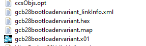
I used some scripts to converts binary file. At the beginnings It was converting 3 different variant which has extensions something like .x01 .x10.,
I moved initialized sections to page 0 and then It converts only .x01 variant not converted like .bin.
I need to fix these problems they really wasted my time too much.
DSP2833x_Headers_nonBIOS.cmd
/*
//###########################################################################
//
// FILE:    DSP2833x_Headers_nonBIOS.cmd
//
// TITLE:   DSP2833x Peripheral registers linker command file
//
// DESCRIPTION:
//
//          This file is for use in Non-BIOS applications.
//
//          Linker command file to place the peripheral structures
//          used within the DSP2833x headerfiles into the correct memory
//          mapped locations.
//
//          This version of the file includes the PieVectorTable structure.
//          For BIOS applications, please use the DSP2833x_Headers_BIOS.cmd file
//          which does not include the PieVectorTable structure.
//
//###########################################################################
*/

MEMORY
{
 PAGE 0:    /* Program Memory */

 PAGE 1:    /* Data Memory */

   DEV_EMU     : origin = 0x000880, length = 0x000180     /* device emulation registers */
   FLASH_REGS  : origin = 0x000A80, length = 0x000060     /* FLASH registers */
   CSM         : origin = 0x000AE0, length = 0x000010     /* code security module registers */

   ADC_MIRROR  : origin = 0x000B00, length = 0x000010     /* ADC Results register mirror */

   XINTF       : origin = 0x000B20, length = 0x000020     /* external interface registers */

   CPU_TIMER0  : origin = 0x000C00, length = 0x000008     /* CPU Timer0 registers */
   CPU_TIMER1  : origin = 0x000C08, length = 0x000008     /* CPU Timer0 registers (CPU Timer1 & Timer2 reserved TI use)*/
   CPU_TIMER2  : origin = 0x000C10, length = 0x000008     /* CPU Timer0 registers (CPU Timer1 & Timer2 reserved TI use)*/

   PIE_CTRL    : origin = 0x000CE0, length = 0x000020     /* PIE control registers */
   PIE_VECT    : origin = 0x000D00, length = 0x000100     /* PIE Vector Table */

   DMA         : origin = 0x001000, length = 0x000200     /* DMA registers */

   MCBSPA      : origin = 0x005000, length = 0x000040     /* McBSP-A registers */
   MCBSPB      : origin = 0x005040, length = 0x000040     /* McBSP-B registers */

   ECANA       : origin = 0x006000, length = 0x000040     /* eCAN-A control and status registers */
   ECANA_LAM   : origin = 0x006040, length = 0x000040     /* eCAN-A local acceptance masks */
   ECANA_MOTS  : origin = 0x006080, length = 0x000040     /* eCAN-A message object time stamps */
   ECANA_MOTO  : origin = 0x0060C0, length = 0x000040     /* eCAN-A object time-out registers */
   ECANA_MBOX  : origin = 0x006100, length = 0x000100     /* eCAN-A mailboxes */

   ECANB       : origin = 0x006200, length = 0x000040     /* eCAN-B control and status registers */
   ECANB_LAM   : origin = 0x006240, length = 0x000040     /* eCAN-B local acceptance masks */
   ECANB_MOTS  : origin = 0x006280, length = 0x000040     /* eCAN-B message object time stamps */
   ECANB_MOTO  : origin = 0x0062C0, length = 0x000040     /* eCAN-B object time-out registers */
   ECANB_MBOX  : origin = 0x006300, length = 0x000100     /* eCAN-B mailboxes */

   EPWM1       : origin = 0x006800, length = 0x000022     /* Enhanced PWM 1 registers */
   EPWM2       : origin = 0x006840, length = 0x000022     /* Enhanced PWM 2 registers */
   EPWM3       : origin = 0x006880, length = 0x000022     /* Enhanced PWM 3 registers */
   EPWM4       : origin = 0x0068C0, length = 0x000022     /* Enhanced PWM 4 registers */
   EPWM5       : origin = 0x006900, length = 0x000022     /* Enhanced PWM 5 registers */
   EPWM6       : origin = 0x006940, length = 0x000022     /* Enhanced PWM 6 registers */

   ECAP1       : origin = 0x006A00, length = 0x000020     /* Enhanced Capture 1 registers */
   ECAP2       : origin = 0x006A20, length = 0x000020     /* Enhanced Capture 2 registers */
   ECAP3       : origin = 0x006A40, length = 0x000020     /* Enhanced Capture 3 registers */
   ECAP4       : origin = 0x006A60, length = 0x000020     /* Enhanced Capture 4 registers */
   ECAP5       : origin = 0x006A80, length = 0x000020     /* Enhanced Capture 5 registers */
   ECAP6       : origin = 0x006AA0, length = 0x000020     /* Enhanced Capture 6 registers */

   EQEP1       : origin = 0x006B00, length = 0x000040     /* Enhanced QEP 1 registers */
   EQEP2       : origin = 0x006B40, length = 0x000040     /* Enhanced QEP 2 registers */

   GPIOCTRL    : origin = 0x006F80, length = 0x000040     /* GPIO control registers */
   GPIODAT     : origin = 0x006FC0, length = 0x000020     /* GPIO data registers */
   GPIOINT     : origin = 0x006FE0, length = 0x000020     /* GPIO interrupt/LPM registers */

   SYSTEM      : origin = 0x007010, length = 0x000020     /* System control registers */
   SPIA        : origin = 0x007040, length = 0x000010     /* SPI-A registers */
   SCIA        : origin = 0x007050, length = 0x000010     /* SCI-A registers */
   XINTRUPT    : origin = 0x007070, length = 0x000010     /* external interrupt registers */

   ADC         : origin = 0x007100, length = 0x000020     /* ADC registers */

   SCIB        : origin = 0x007750, length = 0x000010     /* SCI-B registers */

   SCIC        : origin = 0x007770, length = 0x000010     /* SCI-C registers */

   I2CA        : origin = 0x007900, length = 0x000040     /* I2C-A registers */

   CSM_PWL     : origin = 0x33FFF8, length = 0x000008     /* Part of FLASHA.  CSM password locations. */

   PARTID      : origin = 0x380090, length = 0x000001     /* Part ID register location */
}


SECTIONS
{
   PieVectTableFile : > PIE_VECT,   PAGE = 1

/*** Peripheral Frame 0 Register Structures ***/
   DevEmuRegsFile    : > DEV_EMU,     PAGE = 1
   FlashRegsFile     : > FLASH_REGS,  PAGE = 1
   CsmRegsFile       : > CSM,         PAGE = 1
   AdcMirrorFile     : > ADC_MIRROR,  PAGE = 1
   XintfRegsFile     : > XINTF,       PAGE = 1
   CpuTimer0RegsFile : > CPU_TIMER0,  PAGE = 1
   CpuTimer1RegsFile : > CPU_TIMER1,  PAGE = 1
   CpuTimer2RegsFile : > CPU_TIMER2,  PAGE = 1
   PieCtrlRegsFile   : > PIE_CTRL,    PAGE = 1
   DmaRegsFile       : > DMA,         PAGE = 1

/*** Peripheral Frame 3 Register Structures ***/
   McbspaRegsFile    : > MCBSPA,      PAGE = 1
   McbspbRegsFile    : > MCBSPB,      PAGE = 1

/*** Peripheral Frame 1 Register Structures ***/
   ECanaRegsFile     : > ECANA,       PAGE = 1
   ECanaLAMRegsFile  : > ECANA_LAM    PAGE = 1
   ECanaMboxesFile   : > ECANA_MBOX   PAGE = 1
   ECanaMOTSRegsFile : > ECANA_MOTS   PAGE = 1
   ECanaMOTORegsFile : > ECANA_MOTO   PAGE = 1

   ECanbRegsFile     : > ECANB,       PAGE = 1
   ECanbLAMRegsFile  : > ECANB_LAM    PAGE = 1
   ECanbMboxesFile   : > ECANB_MBOX   PAGE = 1
   ECanbMOTSRegsFile : > ECANB_MOTS   PAGE = 1
   ECanbMOTORegsFile : > ECANB_MOTO   PAGE = 1

   EPwm1RegsFile     : > EPWM1        PAGE = 1
   EPwm2RegsFile     : > EPWM2        PAGE = 1
   EPwm3RegsFile     : > EPWM3        PAGE = 1
   EPwm4RegsFile     : > EPWM4        PAGE = 1
   EPwm5RegsFile     : > EPWM5        PAGE = 1
   EPwm6RegsFile     : > EPWM6        PAGE = 1

   ECap1RegsFile     : > ECAP1        PAGE = 1
   ECap2RegsFile     : > ECAP2        PAGE = 1
   ECap3RegsFile     : > ECAP3        PAGE = 1
   ECap4RegsFile     : > ECAP4        PAGE = 1
   ECap5RegsFile     : > ECAP5        PAGE = 1
   ECap6RegsFile     : > ECAP6        PAGE = 1

   EQep1RegsFile     : > EQEP1        PAGE = 1
   EQep2RegsFile     : > EQEP2        PAGE = 1

   GpioCtrlRegsFile  : > GPIOCTRL     PAGE = 1
   GpioDataRegsFile  : > GPIODAT      PAGE = 1
   GpioIntRegsFile   : > GPIOINT      PAGE = 1

/*** Peripheral Frame 2 Register Structures ***/
   SysCtrlRegsFile   : > SYSTEM,      PAGE = 1
   SpiaRegsFile      : > SPIA,        PAGE = 1
   SciaRegsFile      : > SCIA,        PAGE = 1
   XIntruptRegsFile  : > XINTRUPT,    PAGE = 1
   AdcRegsFile       : > ADC,         PAGE = 1
   ScibRegsFile      : > SCIB,        PAGE = 1
   ScicRegsFile      : > SCIC,        PAGE = 1
   I2caRegsFile      : > I2CA,        PAGE = 1

/*** Code Security Module Register Structures ***/
   CsmPwlFile        : > CSM_PWL,     PAGE = 1

/*** Device Part ID Register Structures ***/
   PartIdRegsFile    : > PARTID,      PAGE = 1

}


/*
//===========================================================================
// End of file.
//===========================================================================
*/