This thread has been locked.
If you have a related question, please click the "Ask a related question" button in the top right corner. The newly created question will be automatically linked to this question.
Hi all,
I'm having trouble with Flash programming on TMS320F28335.
Now I'm using a C2000 TMS320F28335, and I want to copy the program from Flash to RAM so that the DSP can work stand alone.
However, the DSP does not work when I press the Debug button in Code Composer Studio (CCS) and write the program to the DSP : PWM waveforms cannot be observed when I run the program.
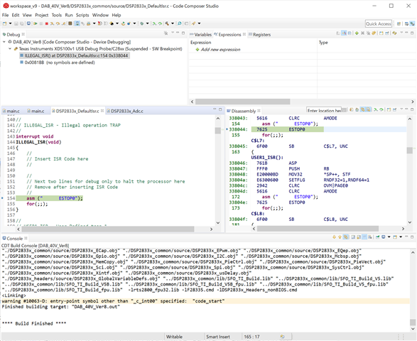
The CCS debug window shows "ILLEGAL_ISR() at DSP2833x_DefaultIsr.c:154 0x338044", but I can't figure out where the problem is.
I attached some picture and the CCS projects that we are currently considering because it is difficult to explain the situation in writing. Please find it.
```
Projects.zip
- DAB_40V_Ver7 : Write to RAM。It works fine.
- DAB_40V_Ver8 : Modify above project to write flash. It cannot work.
Environment1, 2.PNG : Specific environments on CCS
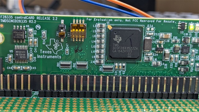
Pin_settings.jpg : A pin settings on control CARD of F28335
Result.PNG : Debug window on CCS
Waveform on GPIO 00 by DAB_40V_ver7.jpg
```
And I used CCS(9.3.0.00012).
I want any advice to fix this issue.
Best Regards,
Eto
This usually occurs when the sections of code that you have declared should run from RAM is called before the memcopy function is ran to copy them over from flash to RAM. Please take a look at this example in C2000Ware, for the correct order of operations for any code you want to run from RAM on a flash loaded project.
C:\ti\c2000\C2000Ware_4_00_00_00\device_support\f2833x\examples\flash_f28335
Let me know if this gets us on the right track.
Another option might be to try not copying over anything to RAM, just executing from flash(even though it is slower than RAM) just to see if we can get that working. This would take the whole memcopy process out of the picture and would show that the flash placement and programming is OK.
Best,
Matthew
I was able to get the program to work. The source code before and after the modification is attached.
Thanks!
---
before:
// DAB-40V-ver6 // 2021/2/5 Yasushi Eto // //########################################################################### // $TI Release: F2833x/F2823x Header Files and Peripheral Examples V142 $ // $Release Date: November 1, 2016 $ // $Copyright: Copyright (C) 2007-2016 Texas Instruments Incorporated - // http://www.ti.com/ ALL RIGHTS RESERVED $ //########################################################################### #include "DSP28x_Project.h" // Device Headerfile and Examples Include File #include <string.h> // Prototype statements for functions found within this file. void EPwm1Config(void); void EPwm2Config(void); void EPwm3Config(void); void EPwm4Config(void); void AdcConfig(void); __interrupt void epwm1_isr(void); // Control method inside #pragma CODE_SECTION(epwm1_isr, "ramfuncs"); extern Uint16 RamfuncsLoadStart; extern Uint16 RamfuncsLoadEnd; extern Uint16 RamfuncsRunStart; extern Uint16 RamfuncsLoadSize; // Global variables used in this example float d; #define PRD 750 // 100kHz int Vo, Vref, pref2; float Sum = 0; // Summation for PI control float e = 0; // error float e2 = 0; // past error float T = 0.00001; // sampling rate 10us float p2, i2, pref; int CMAX = 1000; // countmax int counter = 0; int flag = 0; float Kp = 0.00001; float Ki = 10; // Maximum Dead Band values #define MAX_D 0.5 #define MIN_D 0 void main(void) { // Step 1. Initialize System Control: // PLL, WatchDog, enable Peripheral Clocks // This example function is found in the DSP2833x_SysCtrl.c file. InitSysCtrl(); EALLOW; #if (CPU_FRQ_150MHZ) // Default - 150 MHz SYSCLKOUT #define ADC_MODCLK 0x3 // HSPCLK = SYSCLKOUT/2*ADC_MODCLK2 = 150/(2*3) = 25.0 MHz #endif #if (CPU_FRQ_100MHZ) #define ADC_MODCLK 0x2 // HSPCLK = SYSCLKOUT/2*ADC_MODCLK2 = 100/(2*2) = 25.0 MHz #endif EDIS; // Define ADCCLK clock frequency ( less than or equal to 25 MHz ) // Assuming InitSysCtrl() has set SYSCLKOUT to 150 MHz EALLOW; SysCtrlRegs.HISPCP.all = ADC_MODCLK; EDIS; // Step 2. Initialize GPIO: // This example function is found in the DSP2833x_Gpio.c file and // illustrates how to set the GPIO to it's default state. // InitGpio(); // Skipped for this example // For this case just init GPIO pins for ePWM1, ePWM2, ePWM3 // These functions are in the DSP2833x_EPwm.c file InitEPwm1Gpio(); InitEPwm2Gpio(); InitEPwm3Gpio(); InitEPwm4Gpio(); // Step 3. Clear all interrupts and initialize PIE vector table: // Disable CPU interrupts DINT; // Initialize the PIE control registers to their default state. // The default state is all PIE interrupts disabled and flags // are cleared. // This function is found in the DSP2833x_PieCtrl.c file. InitPieCtrl(); // Disable CPU interrupts and clear all CPU interrupt flags: IER = 0x0000; IFR = 0x0000; // Initialize the PIE vector table with pointers to the shell Interrupt // Service Routines (ISR). // This will populate the entire table, even if the interrupt // is not used in this example. This is useful for debug purposes. // The shell ISR routines are found in DSP2833x_DefaultIsr.c. // This function is found in DSP2833x_PieVect.c. InitPieVectTable(); // Interrupts that are used in this example are re-mapped to // ISR functions found within this file. EALLOW; // This is needed to write to EALLOW protected registers PieVectTable.EPWM1_INT = &epwm1_isr; EDIS; // This is needed to disable write to EALLOW protected registers // Step 4. Initialize all the Device Peripherals: // This function is found in DSP2833x_InitPeripherals.c // InitPeripherals(); // Not required for this example InitAdc(); AdcConfig(); EALLOW; SysCtrlRegs.PCLKCR0.bit.TBCLKSYNC = 0; EDIS; EPwm1Config(); // S1S3 EPwm2Config(); // S2S4 EPwm3Config(); // S5S7 EPwm4Config(); // S6S8 EALLOW; SysCtrlRegs.PCLKCR0.bit.TBCLKSYNC = 1; EDIS; // Step 5. User specific code, enable interrupts memcpy(&RamfuncsRunStart,&RamfuncsLoadStart,(size_t)&RamfuncsLoadSize); InitFlash(); // Enable CPU INT3 which is connected to EPWM1 INT: IER |= M_INT3; // Enable EPWM INTn in the PIE: Group 1 interrupt 1 PieCtrlRegs.PIEIER3.bit.INTx1 = 1; // Enable global Interrupts and higher priority real-time debug events: EINT; // Enable Global interrupt INTM ERTM; // Enable Global realtime interrupt DBGM pref = -37.0; // Direct reference // Step 6. IDLE loop. Just sit and loop forever (optional): for(;;) { } } __interrupt void epwm1_isr(void) { Vo = AdcRegs.ADCRESULT0 >>4; //CT output Vref = AdcRegs.ADCRESULT1 >>4; // CT reference voltage pref2 = AdcRegs.ADCRESULT2 >>4; // Control value from external p2=(1/20.81083)*(Vo-Vref+13); // Sensing Power estimation // pref = (pref2-2047)*0.04; // V1=V2=40V I2=1A // pref = -37.0; // Direct reference (optional) counter = counter + 1; if(counter >= CMAX){ if(flag == 0){ pref = pref+1; flag = 1; }else if (flag == 1){ pref = pref-1; flag = 0; } counter = 0; } // PI control e2 = e; e = pref-p2; // Sum = Sum + (e2 + e)*(3*T/2); Sum = Sum + e*3*T; // Limitter if(Sum > 0.05){ Sum = 0.05; } else if(Sum < -0.05){ Sum = -0.05; } d = Kp*e + Ki*Sum; // d = Kp*e + 0.3; // Limitter if(d > 0.5){ d = 0.5; } else if(d < -0.5){ d =-0.5; } // Describe control method's here... EPwm3Regs.CMPA.half.CMPA = PRD/2+PRD*d/2; EPwm4Regs.CMPA.half.CMPA = PRD/2+PRD*d/2; if(PRD+PRD*d > PRD){ EPwm3Regs.CMPB = PRD*d/2; EPwm4Regs.CMPB = PRD*d/2; } else { EPwm3Regs.CMPB = PRD+PRD*d/2; EPwm4Regs.CMPB = PRD+PRD*d/2; } // Clear INT flag for this timer EPwm1Regs.ETCLR.bit.INT = 1; // Acknowledge this interrupt to receive more interrupts from group 3 PieCtrlRegs.PIEACK.all = PIEACK_GROUP3; } void EPwm1Config() { EPwm1Regs.TBPRD = PRD; // Set timer period -> 100kHz EPwm1Regs.TBPHS.half.TBPHS = 0x0000; // Phase is 0 EPwm1Regs.TBCTR = 0x0000; // Clear counter // Setup TBCLK EPwm1Regs.TBCTL.bit.CTRMODE = TB_COUNT_UP; // Count up EPwm1Regs.TBCTL.bit.PHSEN = TB_DISABLE; // master EPwm1Regs.TBCTL.bit.PRDLD = TB_SHADOW; EPwm1Regs.TBCTL.bit.SYNCOSEL = TB_CTR_ZERO; //EPwm1Regs.TBCTL.bit.HSPCLKDIV = TB_DIV4; // Clock ratio to SYSCLKOUT //EPwm1Regs.TBCTL.bit.CLKDIV = TB_DIV4; EPwm1Regs.CMPCTL.bit.SHDWAMODE = CC_SHADOW; // Load registers every ZERO EPwm1Regs.CMPCTL.bit.SHDWBMODE = CC_SHADOW; EPwm1Regs.CMPCTL.bit.LOADAMODE = CC_CTR_ZERO; EPwm1Regs.CMPCTL.bit.LOADBMODE = CC_CTR_ZERO; // Setup compare EPwm1Regs.CMPA.half.CMPA = PRD/2; //For Duty 50%PWM EPwm1Regs.CMPB = PRD*0.49; //For AdcSoc // Set actions EPwm1Regs.AQCTLA.bit.CAU = AQ_SET; // Set PWM1A on Zero EPwm1Regs.AQCTLA.bit.ZRO = AQ_CLEAR; // 1A:S1 EPwm1Regs.AQCTLB.bit.CAU = AQ_CLEAR; // Set PWM1B on Zero EPwm1Regs.AQCTLB.bit.ZRO = AQ_SET; // 1B:S3 // Deadband EPwm1Regs.DBCTL.bit.OUT_MODE = DB_FULL_ENABLE; // enable Dead-band module EPwm1Regs.DBCTL.bit.POLSEL = DB_ACTV_HIC; // Active Hi complementary EPwm1Regs.DBFED= 38;// FED = 38 TBCLKs -> 0.5us DT @PRD 750 EPwm1Regs.DBRED= 38;// RED = 38 TBCLKs // Interrupt EPwm1Regs.ETSEL.bit.INTSEL = ET_CTRU_CMPA; // Select INT on Zero event EPwm1Regs.ETSEL.bit.INTEN = 1; // Enable INT EPwm1Regs.ETPS.bit.INTPRD = ET_1ST; // Generate INT on 1st event EPwm1Regs.ETSEL.bit.SOCAEN = 1; // Enable SOC on A group EPwm1Regs.ETSEL.bit.SOCASEL = ET_CTRU_CMPB; // Select SOC from from CPMB on upcount. See Fig.44 of ePWM Reference EPwm1Regs.ETPS.bit.SOCAPRD = 1; // Generate INT on 1st event } void EPwm2Config() { EPwm2Regs.TBPRD = PRD; // Set timer period -> 100kHz EPwm2Regs.TBCTR = 0x0000; // Clear counter // Setup TBCLK EPwm2Regs.TBCTL.bit.CTRMODE = TB_COUNT_UP; // Count up EPwm2Regs.TBCTL.bit.PHSEN = TB_ENABLE; // slave move this PWM EPwm2Regs.TBCTL.bit.PRDLD = TB_SHADOW; EPwm2Regs.TBCTL.bit.SYNCOSEL = TB_SYNC_IN; //EPwm2Regs.TBCTL.bit.HSPCLKDIV = TB_DIV4; // Clock ratio to SYSCLKOUT //EPwm2Regs.TBCTL.bit.CLKDIV = TB_DIV4; EPwm2Regs.CMPCTL.bit.SHDWAMODE = CC_SHADOW; // Load registers every ZERO EPwm2Regs.CMPCTL.bit.SHDWBMODE = CC_SHADOW; EPwm2Regs.CMPCTL.bit.LOADAMODE = CC_CTR_ZERO; EPwm2Regs.CMPCTL.bit.LOADBMODE = CC_CTR_ZERO; // Setup compare EPwm2Regs.CMPA.half.CMPA = PRD/2; // Set actions EPwm2Regs.AQCTLA.bit.CAU = AQ_CLEAR; // Set PWM2A on Zero EPwm2Regs.AQCTLA.bit.ZRO = AQ_SET; // 2A:S2 EPwm2Regs.AQCTLB.bit.CAU = AQ_SET; // Set PWM1B on Zero EPwm2Regs.AQCTLB.bit.ZRO = AQ_CLEAR; // 2B:S4 // Deadband EPwm2Regs.DBCTL.bit.OUT_MODE = DB_FULL_ENABLE; // enable Dead-band module EPwm2Regs.DBCTL.bit.POLSEL = DB_ACTV_HIC; // Active Hi complementary EPwm2Regs.DBFED= 38;// FED = 38 TBCLKs -> 0.5us DT @PRD 750 EPwm2Regs.DBRED= 38;// RED = 38 TBCLKs } void EPwm3Config() { EPwm3Regs.TBPRD = PRD; // Set timer period -> 100kHz EPwm3Regs.TBCTR = 0x0000; // Clear counter // Setup TBCLK EPwm3Regs.TBCTL.bit.CTRMODE = TB_COUNT_UP; // Count up EPwm3Regs.TBCTL.bit.PHSEN = TB_ENABLE; // slave move this PWM EPwm3Regs.TBCTL.bit.PRDLD = TB_SHADOW; EPwm3Regs.TBCTL.bit.SYNCOSEL = TB_SYNC_IN; //EPwm3Regs.TBCTL.bit.HSPCLKDIV = TB_DIV4; // Clock ratio to SYSCLKOUT //EPwm3Regs.TBCTL.bit.CLKDIV = TB_DIV4; EPwm3Regs.CMPCTL.bit.SHDWAMODE = CC_SHADOW; // Load registers every ZERO EPwm3Regs.CMPCTL.bit.SHDWBMODE = CC_SHADOW; EPwm3Regs.CMPCTL.bit.LOADAMODE = CC_CTR_ZERO; EPwm3Regs.CMPCTL.bit.LOADBMODE = CC_CTR_ZERO; // Setup compare EPwm3Regs.CMPA.half.CMPA = PRD/2; // Set actions EPwm3Regs.AQCTLA.bit.CAU = AQ_SET; // Set PWM2A on Zero EPwm3Regs.AQCTLA.bit.CBU = AQ_CLEAR; // 2A:S5 EPwm3Regs.AQCTLB.bit.CAU = AQ_CLEAR; // Set PWM1B on Zero EPwm3Regs.AQCTLB.bit.CBU = AQ_SET; // 2B:S7 // Deadband EPwm3Regs.DBCTL.bit.OUT_MODE = DB_FULL_ENABLE; // enable Dead-band module EPwm3Regs.DBCTL.bit.POLSEL = DB_ACTV_HIC; // Active Hi complementary EPwm3Regs.DBFED= 38;// FED = 38 TBCLKs -> 0.5us DT @PRD 750 EPwm3Regs.DBRED= 38;// RED = 38 TBCLKs } void EPwm4Config() { EPwm4Regs.TBPRD = PRD; // Set timer period -> 100kHz EPwm4Regs.TBCTR = 0x0000; // Clear counter // Setup TBCLK EPwm4Regs.TBCTL.bit.CTRMODE = TB_COUNT_UP; // Count up EPwm4Regs.TBCTL.bit.PHSEN = TB_ENABLE; // slave move this PWM EPwm4Regs.TBCTL.bit.PRDLD = TB_SHADOW; EPwm4Regs.TBCTL.bit.SYNCOSEL = TB_SYNC_IN; //EPwm4Regs.TBCTL.bit.HSPCLKDIV = TB_DIV4; // Clock ratio to SYSCLKOUT //EPwm4Regs.TBCTL.bit.CLKDIV = TB_DIV4; EPwm4Regs.CMPCTL.bit.SHDWAMODE = CC_SHADOW; // Load registers every ZERO EPwm4Regs.CMPCTL.bit.SHDWBMODE = CC_SHADOW; EPwm4Regs.CMPCTL.bit.LOADAMODE = CC_CTR_ZERO; EPwm4Regs.CMPCTL.bit.LOADBMODE = CC_CTR_ZERO; // Setup compare EPwm4Regs.CMPA.half.CMPA = PRD/2; // Set actions EPwm4Regs.AQCTLA.bit.CAU = AQ_CLEAR; // Set PWM2A on Zero EPwm4Regs.AQCTLA.bit.CBU = AQ_SET; // 2A:S6 EPwm4Regs.AQCTLB.bit.CAU = AQ_SET; // Set PWM1B on Zero EPwm4Regs.AQCTLB.bit.CBU = AQ_CLEAR; // 2B:S8 // Deadband EPwm4Regs.DBCTL.bit.OUT_MODE = DB_FULL_ENABLE; // enable Dead-band module EPwm4Regs.DBCTL.bit.POLSEL = DB_ACTV_HIC; // Active Hi complementary EPwm4Regs.DBFED= 38;// FED = 38 TBCLKs -> 0.5us DT @PRD 750 EPwm4Regs.DBRED= 38;// RED = 38 TBCLKs } void AdcConfig(void){ AdcRegs.ADCMAXCONV.all = 0x0003; // Setup 3 conv's on SEQ1 AdcRegs.ADCCHSELSEQ1.bit.CONV00 = 0x0000; // Setup ADCINA0 as 1st SEQ1 conv. AdcRegs.ADCCHSELSEQ1.bit.CONV01 = 0x0001; // Setup ADCINA1 as 2nd SEQ1 conv. AdcRegs.ADCCHSELSEQ1.bit.CONV02 = 0x0002; // Setup ADCINA7 as 3rd SEQ1 conv. ? AdcRegs.ADCTRL2.bit.EPWM_SOCA_SEQ1 = 1;// Enable SOCA from ePWM to start SEQ1 AdcRegs.ADCTRL2.bit.INT_ENA_SEQ1 = 1; // Enable SEQ1 interrupt (every EOS) } //=========================================================================== // No more. //===========================================================================
after:
// DAB-40V-ver6 // 2021/2/5 Yasushi Eto // //########################################################################### // $TI Release: F2833x/F2823x Header Files and Peripheral Examples V142 $ // $Release Date: November 1, 2016 $ // $Copyright: Copyright (C) 2007-2016 Texas Instruments Incorporated - // http://www.ti.com/ ALL RIGHTS RESERVED $ //########################################################################### #include "DSP28x_Project.h" // Device Headerfile and Examples Include File #include <string.h> // Functions that will be run from RAM need to be assigned to // a different section. This section will then be mapped using // the linker cmd file. #pragma CODE_SECTION(epwm1_isr, "ramfuncs"); // Prototype statements for functions found within this file. void EPwm1Config(void); void EPwm2Config(void); void EPwm3Config(void); void EPwm4Config(void); void AdcConfig(void); __interrupt void epwm1_isr(void); // Control method inside extern Uint16 RamfuncsLoadStart; extern Uint16 RamfuncsLoadEnd; extern Uint16 RamfuncsRunStart; extern Uint16 RamfuncsLoadSize; // Global variables used in this example float d; #define PRD 750 // 100kHz int Vo, Vref, pref2; float Sum = 0; // Summation for PI control float e = 0; // error float e2 = 0; // past error float T = 0.00001; // sampling rate 10us float p2, i2, pref; int CMAX = 1000; // countmax int counter = 0; int flag = 0; float Kp = 0.0004; float fi = 30000; float Ki = 0.1; // Maximum Dead Band values #define MAX_D 0.5 #define MIN_D 0 void main(void) { // Step 1. Initialize System Control: // PLL, WatchDog, enable Peripheral Clocks // This example function is found in the DSP2833x_SysCtrl.c file. InitSysCtrl(); EALLOW; #if (CPU_FRQ_150MHZ) // Default - 150 MHz SYSCLKOUT #define ADC_MODCLK 0x3 // HSPCLK = SYSCLKOUT/2*ADC_MODCLK2 = 150/(2*3) = 25.0 MHz #endif #if (CPU_FRQ_100MHZ) #define ADC_MODCLK 0x2 // HSPCLK = SYSCLKOUT/2*ADC_MODCLK2 = 100/(2*2) = 25.0 MHz #endif EDIS; // Define ADCCLK clock frequency ( less than or equal to 25 MHz ) // Assuming InitSysCtrl() has set SYSCLKOUT to 150 MHz EALLOW; SysCtrlRegs.HISPCP.all = ADC_MODCLK; EDIS; // Step 2. Initialize GPIO: // This example function is found in the DSP2833x_Gpio.c file and // illustrates how to set the GPIO to it's default state. // InitGpio(); // Skipped for this example // For this case just init GPIO pins for ePWM1, ePWM2, ePWM3 // These functions are in the DSP2833x_EPwm.c file InitEPwm1Gpio(); InitEPwm2Gpio(); InitEPwm3Gpio(); InitEPwm4Gpio(); // Step 3. Clear all interrupts and initialize PIE vector table: // Disable CPU interrupts DINT; // Initialize the PIE control registers to their default state. // The default state is all PIE interrupts disabled and flags // are cleared. // This function is found in the DSP2833x_PieCtrl.c file. InitPieCtrl(); // Disable CPU interrupts and clear all CPU interrupt flags: IER = 0x0000; IFR = 0x0000; // Initialize the PIE vector table with pointers to the shell Interrupt // Service Routines (ISR). // This will populate the entire table, even if the interrupt // is not used in this example. This is useful for debug purposes. // The shell ISR routines are found in DSP2833x_DefaultIsr.c. // This function is found in DSP2833x_PieVect.c. InitPieVectTable(); // Interrupts that are used in this example are re-mapped to // ISR functions found within this file. EALLOW; // This is needed to write to EALLOW protected registers PieVectTable.EPWM1_INT = &epwm1_isr; EDIS; // This is needed to disable write to EALLOW protected registers // Step 4. Initialize all the Device Peripherals: // This function is found in DSP2833x_InitPeripherals.c // InitPeripherals(); // Not required for this example EALLOW; SysCtrlRegs.PCLKCR0.bit.TBCLKSYNC = 0; EDIS; EPwm1Config(); // S1S3 EPwm2Config(); // S2S4 EPwm3Config(); // S5S7 EPwm4Config(); // S6S8 EALLOW; SysCtrlRegs.PCLKCR0.bit.TBCLKSYNC = 1; EDIS; // Step 5. User specific code, enable interrupts memcpy(&RamfuncsRunStart,&RamfuncsLoadStart,(size_t)&RamfuncsLoadSize); InitFlash(); // Enable CPU INT3 which is connected to EPWM1 INT: IER |= M_INT3; // I'm not sure but if InitAdc() is called faster than PWM config, "ILLEGAL ISR" will be occured. // If "ILLEGAL ISR" occured in InitAdc(), Change the location of the below 2 line InitAdc(); AdcConfig(); // Enable EPWM INTn in the PIE: Group 1 interrupt 1 PieCtrlRegs.PIEIER3.bit.INTx1 = 1; // Enable global Interrupts and higher priority real-time debug events: EINT; // Enable Global interrupt INTM ERTM; // Enable Global realtime interrupt DBGM pref = -37.0; // Direct reference // Step 6. IDLE loop. Just sit and loop forever (optional): for(;;) { } } __interrupt void epwm1_isr(void) { Vo = AdcRegs.ADCRESULT0 >>4; //CT output Vref = AdcRegs.ADCRESULT1 >>4; // CT reference voltage pref2 = AdcRegs.ADCRESULT2 >>4; // Control value from external p2=(0.0477427)*(Vo-Vref+68); // Sensing Power estimation // pref = (pref2-2047)*0.04; // V1=V2=40V I2=1A pref = 13.84; // Direct reference (optional) /* pref d 13.84 0.1 25.51 0.2 32.75 0.3 36.60 0.4 -19.68 -0.1 -30.47 -0.2 -39.84 -0.3 -45.92 -0.4 */ /* counter = counter + 1; if(counter >= CMAX){ if(flag == 0){ pref = pref+1; flag = 1; }else if (flag == 1){ pref = pref-1; flag = 0; } counter = 0; } */ // PI control e2 = e; e = pref-p2; Sum = Sum + (e2 + e)*(T/2); // Sum = Sum + e*T; // Limitter if(Sum > 1.3){ Sum = 1.3; } else if(Sum < -1.3){ Sum = -1.3; } d = Kp*e + Ki*Sum; // d = Kp*e + 0.3; // Limitter if(d > 0.5){ d = 0.5; } else if(d < -0.5){ d =-0.5; } // Describe control method's here... EPwm3Regs.CMPA.half.CMPA = PRD/2+PRD*d/2; EPwm4Regs.CMPA.half.CMPA = PRD/2+PRD*d/2; if(PRD+PRD*d > PRD){ EPwm3Regs.CMPB = PRD*d/2; EPwm4Regs.CMPB = PRD*d/2; } else { EPwm3Regs.CMPB = PRD+PRD*d/2; EPwm4Regs.CMPB = PRD+PRD*d/2; } // Clear INT flag for this timer EPwm1Regs.ETCLR.bit.INT = 1; // Acknowledge this interrupt to receive more interrupts from group 3 PieCtrlRegs.PIEACK.all = PIEACK_GROUP3; } void EPwm1Config() { EPwm1Regs.TBPRD = PRD; // Set timer period -> 100kHz EPwm1Regs.TBPHS.half.TBPHS = 0x0000; // Phase is 0 EPwm1Regs.TBCTR = 0x0000; // Clear counter // Setup TBCLK EPwm1Regs.TBCTL.bit.CTRMODE = TB_COUNT_UP; // Count up EPwm1Regs.TBCTL.bit.PHSEN = TB_DISABLE; // master EPwm1Regs.TBCTL.bit.PRDLD = TB_SHADOW; EPwm1Regs.TBCTL.bit.SYNCOSEL = TB_CTR_ZERO; //EPwm1Regs.TBCTL.bit.HSPCLKDIV = TB_DIV4; // Clock ratio to SYSCLKOUT //EPwm1Regs.TBCTL.bit.CLKDIV = TB_DIV2; EPwm1Regs.CMPCTL.bit.SHDWAMODE = CC_SHADOW; // Load registers every ZERO EPwm1Regs.CMPCTL.bit.SHDWBMODE = CC_SHADOW; EPwm1Regs.CMPCTL.bit.LOADAMODE = CC_CTR_ZERO; EPwm1Regs.CMPCTL.bit.LOADBMODE = CC_CTR_ZERO; // Setup compare EPwm1Regs.CMPA.half.CMPA = PRD/2; //For Duty 50%PWM EPwm1Regs.CMPB = PRD*0.9; //For AdcSoc // Set actions EPwm1Regs.AQCTLA.bit.CAU = AQ_SET; // Set PWM1A on Zero EPwm1Regs.AQCTLA.bit.ZRO = AQ_CLEAR; // 1A:S1 EPwm1Regs.AQCTLB.bit.CAU = AQ_CLEAR; // Set PWM1B on Zero EPwm1Regs.AQCTLB.bit.ZRO = AQ_SET; // 1B:S3 // Deadband EPwm1Regs.DBCTL.bit.OUT_MODE = DB_FULL_ENABLE; // enable Dead-band module EPwm1Regs.DBCTL.bit.POLSEL = DB_ACTV_HIC; // Active Hi complementary EPwm1Regs.DBFED= 38;// FED = 38 TBCLKs -> 0.5us DT @PRD 750 EPwm1Regs.DBRED= 38;// RED = 38 TBCLKs // Interrupt EPwm1Regs.ETSEL.bit.INTSEL = ET_CTRU_CMPB; // Select INT on Zero event EPwm1Regs.ETSEL.bit.INTEN = 1; // Enable INT EPwm1Regs.ETPS.bit.INTPRD = ET_1ST; // Generate INT on 1st event EPwm1Regs.ETSEL.bit.SOCAEN = 1; // Enable SOC on A group EPwm1Regs.ETSEL.bit.SOCASEL = ET_CTR_ZERO; // Select SOC from from CPMB on upcount. See Fig.44 of ePWM Reference EPwm1Regs.ETPS.bit.SOCAPRD = ET_1ST; // Generate INT on 1st event } void EPwm2Config() { EPwm2Regs.TBPRD = PRD; // Set timer period -> 100kHz EPwm2Regs.TBCTR = 0x0000; // Clear counter // Setup TBCLK EPwm2Regs.TBCTL.bit.CTRMODE = TB_COUNT_UP; // Count up EPwm2Regs.TBCTL.bit.PHSEN = TB_ENABLE; // slave move this PWM EPwm2Regs.TBCTL.bit.PRDLD = TB_SHADOW; EPwm2Regs.TBCTL.bit.SYNCOSEL = TB_SYNC_IN; //EPwm2Regs.TBCTL.bit.HSPCLKDIV = TB_DIV4; // Clock ratio to SYSCLKOUT //EPwm2Regs.TBCTL.bit.CLKDIV = TB_DIV2; EPwm2Regs.CMPCTL.bit.SHDWAMODE = CC_SHADOW; // Load registers every ZERO EPwm2Regs.CMPCTL.bit.SHDWBMODE = CC_SHADOW; EPwm2Regs.CMPCTL.bit.LOADAMODE = CC_CTR_ZERO; EPwm2Regs.CMPCTL.bit.LOADBMODE = CC_CTR_ZERO; // Setup compare EPwm2Regs.CMPA.half.CMPA = PRD/2; // Set actions EPwm2Regs.AQCTLA.bit.CAU = AQ_CLEAR; // Set PWM2A on Zero EPwm2Regs.AQCTLA.bit.ZRO = AQ_SET; // 2A:S2 EPwm2Regs.AQCTLB.bit.CAU = AQ_SET; // Set PWM1B on Zero EPwm2Regs.AQCTLB.bit.ZRO = AQ_CLEAR; // 2B:S4 // Deadband EPwm2Regs.DBCTL.bit.OUT_MODE = DB_FULL_ENABLE; // enable Dead-band module EPwm2Regs.DBCTL.bit.POLSEL = DB_ACTV_HIC; // Active Hi complementary EPwm2Regs.DBFED= 38;// FED = 38 TBCLKs -> 0.5us DT @PRD 750 EPwm2Regs.DBRED= 38;// RED = 38 TBCLKs } void EPwm3Config() { EPwm3Regs.TBPRD = PRD; // Set timer period -> 100kHz EPwm3Regs.TBCTR = 0x0000; // Clear counter // Setup TBCLK EPwm3Regs.TBCTL.bit.CTRMODE = TB_COUNT_UP; // Count up EPwm3Regs.TBCTL.bit.PHSEN = TB_ENABLE; // slave move this PWM EPwm3Regs.TBCTL.bit.PRDLD = TB_SHADOW; EPwm3Regs.TBCTL.bit.SYNCOSEL = TB_SYNC_IN; //EPwm3Regs.TBCTL.bit.HSPCLKDIV = TB_DIV4; // Clock ratio to SYSCLKOUT //EPwm3Regs.TBCTL.bit.CLKDIV = TB_DIV2; EPwm3Regs.CMPCTL.bit.SHDWAMODE = CC_SHADOW; // Load registers every ZERO EPwm3Regs.CMPCTL.bit.SHDWBMODE = CC_SHADOW; EPwm3Regs.CMPCTL.bit.LOADAMODE = CC_CTR_ZERO; EPwm3Regs.CMPCTL.bit.LOADBMODE = CC_CTR_ZERO; // EPwm3Regs.CMPCTL.bit.SHDWAMODE = 1; // Load registers in realtime // EPwm3Regs.CMPCTL.bit.SHDWBMODE = 1; // Setup compare EPwm3Regs.CMPA.half.CMPA = PRD/2; // Set actions EPwm3Regs.AQCTLA.bit.CAU = AQ_SET; // Set PWM2A on Zero EPwm3Regs.AQCTLA.bit.CBU = AQ_CLEAR; // 2A:S5 EPwm3Regs.AQCTLB.bit.CAU = AQ_CLEAR; // Set PWM1B on Zero EPwm3Regs.AQCTLB.bit.CBU = AQ_SET; // 2B:S7 // Deadband EPwm3Regs.DBCTL.bit.OUT_MODE = DB_FULL_ENABLE; // enable Dead-band module EPwm3Regs.DBCTL.bit.POLSEL = DB_ACTV_HIC; // Active Hi complementary EPwm3Regs.DBFED= 38;// FED = 38 TBCLKs -> 0.5us DT @PRD 750 EPwm3Regs.DBRED= 38;// RED = 38 TBCLKs } void EPwm4Config() { EPwm4Regs.TBPRD = PRD; // Set timer period -> 100kHz EPwm4Regs.TBCTR = 0x0000; // Clear counter // Setup TBCLK EPwm4Regs.TBCTL.bit.CTRMODE = TB_COUNT_UP; // Count up EPwm4Regs.TBCTL.bit.PHSEN = TB_ENABLE; // slave move this PWM EPwm4Regs.TBCTL.bit.PRDLD = TB_SHADOW; EPwm4Regs.TBCTL.bit.SYNCOSEL = TB_SYNC_IN; //EPwm4Regs.TBCTL.bit.HSPCLKDIV = TB_DIV4; // Clock ratio to SYSCLKOUT //EPwm4Regs.TBCTL.bit.CLKDIV = TB_DIV2; EPwm3Regs.CMPCTL.bit.SHDWAMODE = CC_SHADOW; // Load registers every ZERO EPwm3Regs.CMPCTL.bit.SHDWBMODE = CC_SHADOW; EPwm3Regs.CMPCTL.bit.LOADAMODE = CC_CTR_ZERO; EPwm3Regs.CMPCTL.bit.LOADBMODE = CC_CTR_ZERO; // EPwm3Regs.CMPCTL.bit.SHDWAMODE = 1; // Load registers in realtime // EPwm3Regs.CMPCTL.bit.SHDWBMODE = 1; // Setup compare EPwm4Regs.CMPA.half.CMPA = PRD/2; // Set actions EPwm4Regs.AQCTLA.bit.CAU = AQ_CLEAR; // Set PWM2A on Zero EPwm4Regs.AQCTLA.bit.CBU = AQ_SET; // 2A:S6 EPwm4Regs.AQCTLB.bit.CAU = AQ_SET; // Set PWM1B on Zero EPwm4Regs.AQCTLB.bit.CBU = AQ_CLEAR; // 2B:S8 // Deadband EPwm4Regs.DBCTL.bit.OUT_MODE = DB_FULL_ENABLE; // enable Dead-band module EPwm4Regs.DBCTL.bit.POLSEL = DB_ACTV_HIC; // Active Hi complementary EPwm4Regs.DBFED= 38;// FED = 38 TBCLKs -> 0.5us DT @PRD 750 EPwm4Regs.DBRED= 38;// RED = 38 TBCLKs } void AdcConfig(void){ AdcRegs.ADCMAXCONV.all = 0x0003; // Setup 3 conv's on SEQ1 AdcRegs.ADCCHSELSEQ1.bit.CONV00 = 0x0000; // Setup ADCINA0 as 1st SEQ1 conv. AdcRegs.ADCCHSELSEQ1.bit.CONV01 = 0x0001; // Setup ADCINA1 as 2nd SEQ1 conv. AdcRegs.ADCCHSELSEQ1.bit.CONV02 = 0x0002; // Setup ADCINA7 as 3rd SEQ1 conv. ? AdcRegs.ADCTRL2.bit.EPWM_SOCA_SEQ1 = 1;// Enable SOCA from ePWM to start SEQ1 AdcRegs.ADCTRL2.bit.INT_ENA_SEQ1 = 1; // Enable SEQ1 interrupt (every EOS) } //=========================================================================== // No more. //===========================================================================