This thread has been locked.

If you have a related question, please click the "Ask a related question" button in the top right corner. The newly created question will be automatically linked to this question.

TMS320F28027: Low-level output sink current: static or dynamic characteristic?

Part Number: TMS320F28027

Dear,

We have an application in which a TMS320 microcontroller is communicating with a sensor over I2C. The SDA and SCL pin are connected to a first order RC low pass filter, to slow down the fall time of these signals. This is shown on the schematic below.
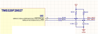
 

When the I2C signals are switching from high to low, the capacitance (C200/C201) which is charged to 3.3V will start to discharge. Therefore, a transient current will flow which is limited by the series resistor (R200/R201). Next, as long as the signal is kept low, a static current will flow which is limited by both the pull-up resistor (R203/R205) and the series resistor. The static current would be (3.3V-Vol)/(R203+R200) in case of SDA.

The question I now have is about the low-level output sink current. The datasheet of the TMS320 states the maximum value for this sink current. Is this a static characteristic, as in when the signal is kept low? Or should the maximum sink current also be obeyed for the transient current, as when the signal is switching from high to low?

In other words, when dimensioning R200 and R203 (in case of SDA) should I make sure that R200 is big enough so that, when discharging the capacitor, the current stays below the maximum sinking current? Or is it enough to make sure that the static current of (3.3V-Vol)/(R203+R200) stays below the maximum sinking current?

I would assume that it is as static characteristic, in the sense that it is the power dissipated by the source-drain resistance inside the TMS320 device that heats up and would cause damage to the device when a current higher than the maximum sinking current is flowing. As it would be a heating phenomenon, a short transient current overload would not cause any damage.

Is there someone who can answer this or point me in the right direction?


Kind regards,
Steven.

  • Hi Kevin,

    Thank you for the reply. I have read the post you pointed too but I could not find the answer there. I would like to understand if the maximum sink current is important because of the heating of the internal source-drain resistance, or if there are other reasons.

    Also, as an extra remark in the above schematic there is a discrete capacitor which will cause peak currents when switching. However, if we would remove these discrete capacitors then there is still "parasitic" capacitance of e.g. the I2C traces on the PCB. So even without these discrete caps, a peak current higher than the maximum sink current will exist except if a rather large (around 1K) resistor is chosen for R200/R201. I do not think that the latter is commonly done.


    Kind regards,
    Steven.

  • Steven,

    Thanks for the question, you're paying attention to the details!  Short answer is your circuit will be fine for I2C.  The ratings in the Datasheet Recommended Operating Conditions table are DC ratings, not transient.  The transient current to charge the net capacitance will peak higher than this and is normally no issue.  The exception would be if this was an exceptionally large capacitor and the signal was switching at a high frequency so you ended up with an RMS current of around the DC rated value.  I doubt you're anywhere near that, and as long as you have some nominal series resistance it will be self limiting.

    Normally I'd suggest only using a series resistor and the parasitic capacitance to slow down edge rates rather than a discrete capacitor on the signal.  Reason being the capacitor 1) creates higher currents (EMI) and power and 2) slow edges can be more susceptible to noise around the Vih/Vil of the receiver on the far end of line (depending on where the capacitor is placed in the transmission line).  But, this can still work if you're careful; you can always depop the capacitor if you see issues.

    Good luck and best regards,

    Jason

  • Hi Jason,

    Thank you for your answer. Your explanation about the transient current is very clear.

    I first used a higher value series resistor so that the small trace capacitance was sufficient to get the desired RC constant. I changed this however because I am worried that the variation
    in trace capacitance between different boards (in production) would be too large. I am using an FR4 PCB for this design and if the trace capacitance would differ too much between boards, for some boards the rise/fall time specifications may be violated. Therefore, I dimensioned the discrete capacitor so that it is approximately an order of magnitude bigger than the trace capacitance. In this way the variations in trace capacitance between boards would have less impact on the rise/fall time. The discrete capacitance uses a cap with 1% tolerance. The value of the series resistor was lowered so that, with the higher capacitance, the RC constant would remain the same.

    Do you think that the above is a valid reasoning?

    You also mentioned in your answer that "2) slow edges can be more susceptible to noise around the Vih/Vil of the receiver on the far end of line (depending on where the capacitor is placed in the transmission line)". Could you elaborate on this? I am afraid that I do not fully understand what was meant by that.


    Kind regards,
    Steven.

  • Steven,

    Your approach seems reasonable, esp. if you have strict fall time requirements to meet (rise time will anyway be slow).  What is the receiver device you are interfacing to, or is this a general requirement?

    An input buffer for a receiver may/may not have hysteresis  built in.  This video describes the mechanism (for a comparator, but same principle applies):

    https://training.ti.com/ti-precision-labs-comparator-how-solve-comparator-noise-problems-hysteresis

    If the input voltage moves slowly between the Vih/Vil of the input buffer (an undefined region) AND there is noise coupled on to the line then this could be seen as multiple transitions to the receiver.  Slower rise/fall times are more susceptible to noise glitches since they spend more time in the gray zone.  Most I2C devices have internal glitch filtering so this is probably not an issue for you, it is just a general principle to not slow down edges too much, especially if there is a long or high impedance signal source.

    Best regards,

    Jason

  • Jason,

    Thank you for the extra explanation and the additional reference, I now understand.

    With respect to the timing requirements, I am following I2C fast-mode (and 3.3V Vdd) giving a fall time requirement of 12-300ns and a rise time requirement of 20-300ns. The receiver I am interfacing to is a sensor. I think "the challenge" is to keep the fall time above 12ns, with the rise time under 300ns, with the voltage over the series resistor as low as possible and all of this not much depending on differences in trace capacitance.

    Kind regards,
    Steven.