Other Parts Discussed in Thread: MOTORWARE, CONTROLSUITE
- What I am trying to do : Run 3-phase Induction motor using Direct Torque Control method.
- What I am sensing: 3-phase stator currents through current sensor board and speed through speed encoder.

- MCU: TI C2000 F29069M
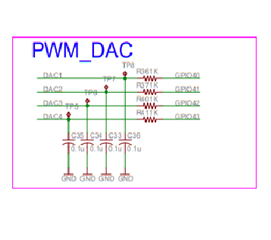
- Level Shifter : 2.5 shift, 0.5 gain
- Current sensor : 0.1 gain
- The issue: Significant jumps in current retrieved and seen through DAC, even if the voltage supply is not given.
-
Waveforms shown below:
- Yellow : Phase A current retrieved and seen through DAC
- Green : Phase B current in DAC
- Blue : Phase C current in DAC
- Pink : Phase A actual current sensed by current probe
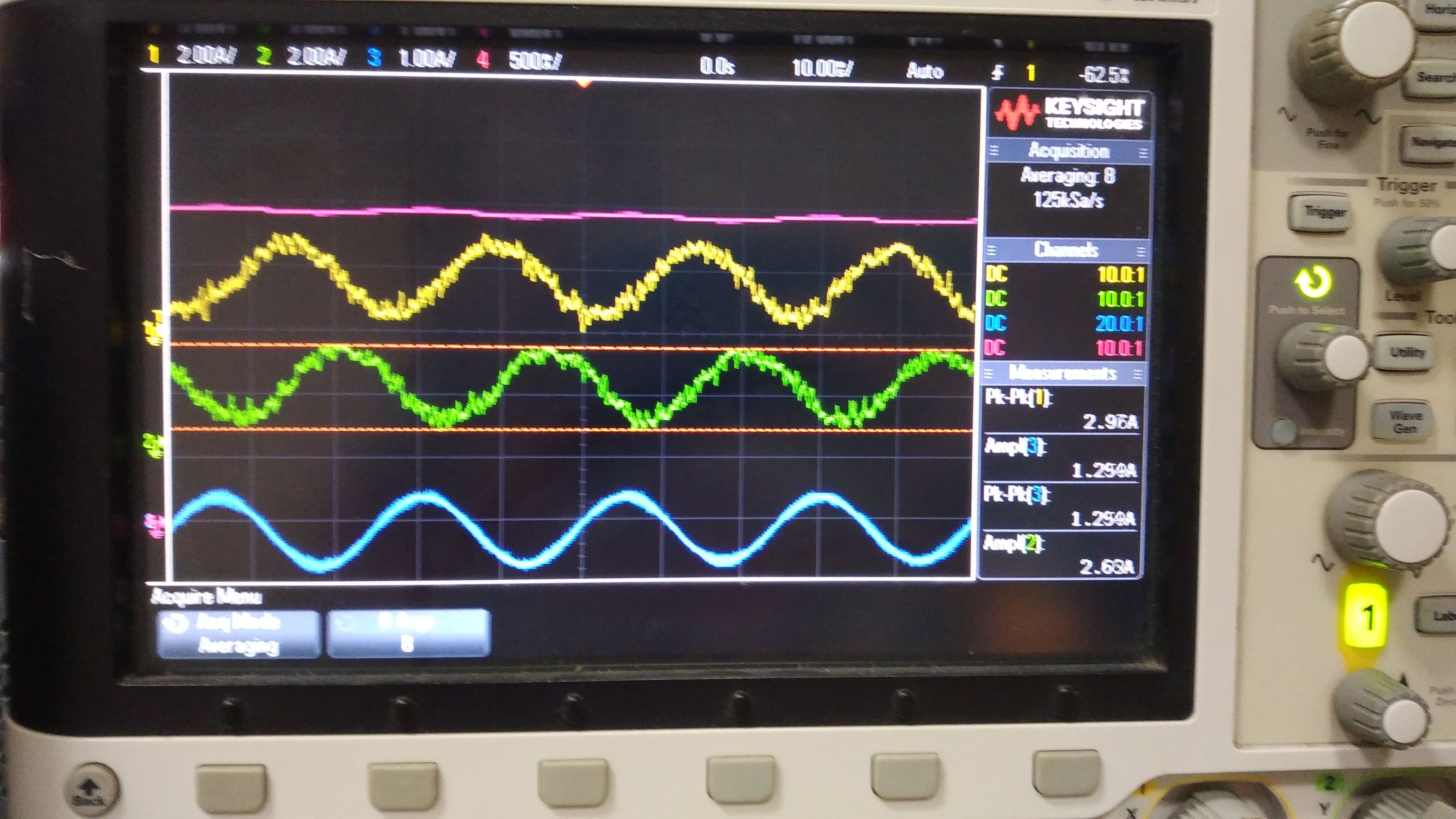
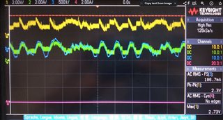
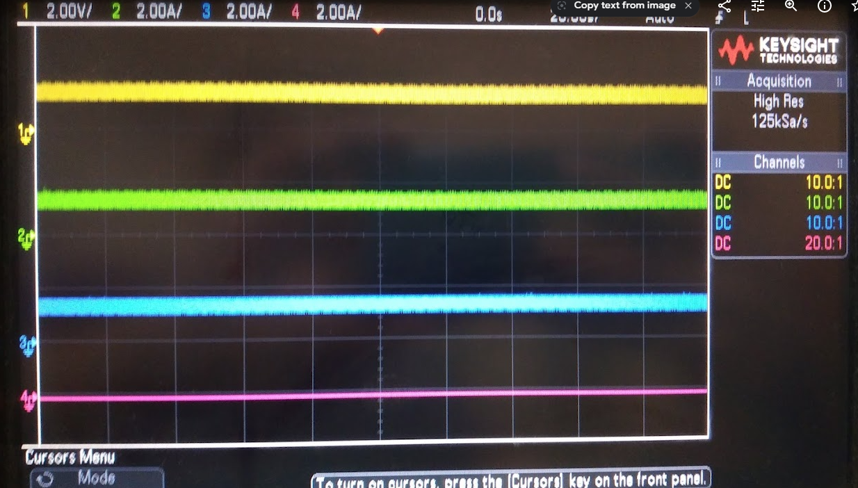
- Fig 1. Only shift seen in DAC as the code is not yet turned on.
-
Fig 1. Only the shift of level shifter seen in DAc as code not yet started.
Fig 2 Below shown when the inverter switching is started, these jumps are seen in the phase currents 1. 2. & 3 waveforms .
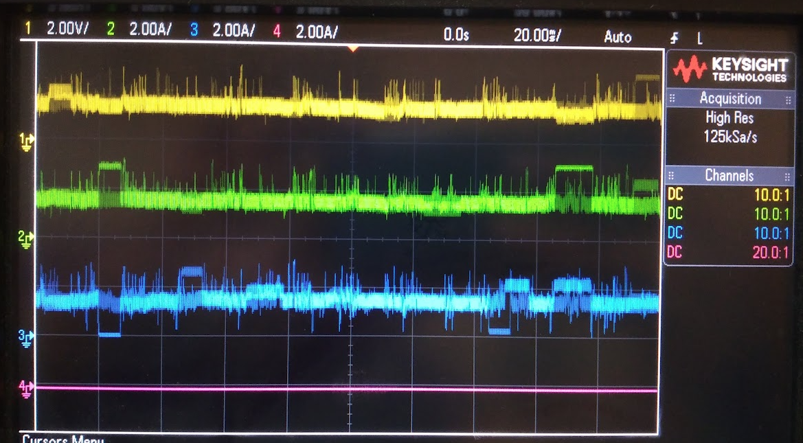
Fig .2 Jumps in current even though supply is off
- Fig 3. When supply is given, the first three waves (phase A, B, C currents) are not sine wave as they should come as the 4th waveform (pink). 4th waveform is the phase A current through current probe.

- Another issue I am facing is that the speed encoder is not giving some constant value of speed while running the motor. It is varying a lot by +-30 to 40 rpm which is affecting the speed control PI loop as well. Is it because of the encoder fault or in my code some problem is there?
- I am attaching the .c code and also the video of current waveform and how the encoder result is varying. Please do take a look.
- DTC_code_in_the_making_running.rar
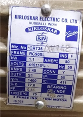
// ------------------ DTC Trial ------------------------ /* ------------------- External Connections : ---------------- 1. Eqep: From encoder ---> to ---> DSP board Ch. A ---> pin 45 gpio 20 Ch B. ---> pin 48 gpio 21 Ch I. ---> pin 49 gpio 23 2. To monitor speed on DSO DAC : Epwm 8A : speed in rpm : pin 72 3. Current Sensing FRom current sensor ---> to ---> ADC ports on board Ia_sense (I4 from sensor) ----> pin 69 [ ADC INA4] Ib_sense (I3 from sensor) ----> pin 25 [ ADC INA2] Ic_sense (I2 from sensor) ----> pin 27 [ ADC INA0] ** To see above currents retrieved ** DAC connections Ia seen at ------------------- Calculations ---------------------- 1. TBPRD : For assymmetric : TBPRD = (fclk/fsw)-1 For up-down mode: TBPRD = (fclk/2*fsw) ......... Symmetric PWM So for EPWM_TIMER_TBPRD : fclk = 90 MHz ; fsw = 5 kHz = (90e6)/(2*5e3) EPWM_TIMER_TBPRD = 9000 So for EPWM_TIMER_TBPRD : fclk = 90 MHz ; fsw = 10 kHz = (90e6)/(2*10e3) EPWM_TIMER_TBPRD = 4500 2. Motor Rating: P = 1.1 kW ; I_rated = 2.45 A ; Nr = 1400 rpm ; %n = 77% ; 0.81 pf i] Rated Torque: Te = P/w = 1.1e3/ 2.pi.Nr = 1.1e3/ (2.pi.1400/60) Te = 7.50301 Nm */ //########################################################################### // // Included Files // #include "DSP28x_Project.h" // Device Headerfile and Examples Include File #include "math.h" // // Function Prototypes // void InitEPwm7Example(void); void InitEPwm8Example(void); void InitEPwm1Example(void); void InitEPwm2Example(void); void InitEPwm3Example(void); __interrupt void epwm7_isr(void); void Adc_Config(void) ; // speed meas initialization void POSSPEED_Calc() ; void POSSPEED_Init() ; // abc-to-alpha_beta transformation void i_transformation() ; void v_transformation() ; void V_test_new() ; // Phase voltage computation void sectorselect() ; void v_phase_generation() ; // Defines that configure the period for each timer // // Trial 1: Timing info for 10KHz #define EPWM7_TIMER_TBPRD 4500 // Period register 10kHz signal up down count mode #define EPWM1_TIMER_TBPRD 4500 // Period register #define Ts 0.000222 // 1/TBPRD //sampling time i.e. 1/TBPRD #define inc 7.8E-6//0.1 // Trial 2: Timing info for 5KHz /* #define EPWM7_TIMER_TBPRD 9000 #define EPWM1_TIMER_TBPRD 9000 #define inc 15.6E-6 */ int DAC = 1 ; // Defines to keep track of which way the compare value is moving double REF_A=0, REF_B=0, REF_C=0 ; double Theta=0,del_Theta=0.0314,A,B,C; int interupt=0;//0.0279*0.05 float Freq=50,Vm=2250,m=0; Uint16 index=1,PWM=0; // speed sensing variables unsigned int current_pos=0, current_time, time=0; float w_rpm=0, Positive_t_speed = 0, Negative_t_speed=0; // Speed Controller function void speed_controller() ; //float w_ref=1000, Kp=1, Ki=1 ; float Kp= 0.0075, Ki= 0.25 ; int wm_control = 0 ; float w_error = 0, w_ref = 0.01, w_rpm_pu = 0 ; float integrator_w = 0, pi_op = 0 ; float Te_max = 7.5 ; // sat lim for PI controller /* float integrator_satlim = 1000+20; // w_ref + buffer int wm_control = 0 ; // control expressiom to turn on speed control loop float w_error_past=0 , integrator_past=0; // past value of i/p and integrator float w_error_pres = 0, integrator_pres=0; // present values of input and integrator float w_new=0; // o/p of PI controller */ // Speed filter variables : float w_rpm_filter_pres=0, w_rpm_filter_past=0, w_rpm_pres=0, w_rpm_past=0 ; //float a1 = 0.9691, a2 = 0.01547; // 50 Hz fc float a1 = 0.9813, a2 = 0.009337; // 30 Hz fc //float a1 = 0.9969, a2 = 0.001568; // 5 Hz fc //float a1 = 0.9956, a2 = 0.002217; // 5 Hz fc a*root 2 // 3-phase terms : currents and voltages variable int P=4; // Num of poles double Ia_sense=0, Ib_sense=0, Ic_sense=0; // motor currents 3 ph from ADC ports float Ia=0, Ib=0, Ic=0; // Retrieved signals float Ia_offset= 3105 ,Ib_offset=3090, Ic_offset=3085, Ia_scale=0.012 ,Ib_scale=0.011,Ic_scale=0.02; double Isalpha=0; double Isbeta=0; float Vdc= 100, Vdc_sense=0, Vdc_pu=0; // DC Link voltage float Vdc_offset=0, Vdc_scale=0 ; // DC Link vtg offset and scaling factor double Vsalpha=0; double Vsbeta=0; // Switching function for phase voltage float Vao=0 , Vbo = 0, Vco = 0 ; // Pole voltages float Vcm=0 ; // Common Mode vtgs float Van=0, Vbn=0, Vcn=0 ; // Phase voltages float Sa=0 , Sb=0, Sc=0 ; // switching function logic float S1=0 , S2=0, S3=0, S4=0, S5=0, S6=0, S7=0 ; // Vector number int vtg_vector=0, vtg_vector_test = 0 ; // vector number from LUT // To check phase voltage manually float theta_el = 0; // Flux and Torque estimation // Flux, Torque , theta equation calculation functions void Te_psi_estimation(); float Rs =0.00765 ; // Flux float psi_s=0 ; double psi_salpha=0, psi_sbeta=0; double psi_theta=0 ; double psi_salpha_offset = 0, psi_sbeta_offset = 0 ; double psi_salpha_avg = 0, psi_salpha_acc = 0, count = 1 ; double psi_sbeta_avg = 0 , psi_sbeta_acc = 0 ; double psi_salpha_new = 0 , psi_sbeta_new = 0 ; // Torque double Te = 0 ; // Flux and Torque Hysteresis controller // Flux hysteresis comparator void flux_hys_comparator(); double psi_ref = 0.5 , psi_actual= 0, psi_band = 0.001, psi_error = 0; int d_psi = 0 ; // Torque hys comparator void Te_hys_comparator(); double Te_ref= 0, Te_actual= 0, Te_band=0.1 /*0.37515*/, Te_error = 0 ; int d_Te=0 ; // Lookup Table void LUT() ; int sector = 0; __interrupt void epwm7_isr(void) { // ---------------- Currents sensing and scaling ----------------- Ia_sense = AdcResult.ADCRESULT0; // Phase a current Ib_sense = AdcResult.ADCRESULT1; // Phase b current Ic_sense = AdcResult.ADCRESULT2; // Phase c current // ** Note : Above are all scaled and shifted values due to sensor and shifter // ------------------ DC voltage Sensing -------------------------- Vdc_sense = AdcResult.ADCRESULT3; /*=================Original Signal Retrieval====================== **Here since our actual input is bipolar signal(say sine wave), we need to use level shifter to convert that to uni-polar >> Then retrieve the original signal >> */ Ia = (Ia_sense - Ia_offset)*(Ia_scale) ; Ib = (Ib_sense - Ib_offset)*(Ib_scale) ; Ic = (Ic_sense - Ic_offset)*(Ic_scale) ; // Vdc = (Vdc_sense - Vdc_offset)*Vdc_scale*Vdc_pu ; // Current transformation function i_transformation() ; // Phase Voltage computation /* if(theta_el>=0 && theta_el<360) { theta_el += 1.8 ; //theta_el=theta_el+6.28 ; { if(theta_el >= 360) { theta_el = 0 ; } } } */ v_phase_generation() ; //V_test_new() ; // Voltage transformation v_transformation() ; Te_psi_estimation() ; // sectorselect(); flux_hys_comparator() ; // Flux hysteresis comparator // For speed measurment POSSPEED_Calc(); w_rpm=(659180)/time; Positive_t_speed=2000+w_rpm; Negative_t_speed=2000-w_rpm; // Spped filter + controller function speed_controller() ; Te_hys_comparator() ; // Torque hysteresis comparator sectorselect() ; // to get vtg_vector value LUT() ; // Lookup table // To see the original current obtained above and compare with the actual one // Configuring to DAC // To see currents retrieved if(DAC == 1) { EPwm7Regs.CMPA.half.CMPA = (Ia*500)+2250 ; //(Ia*2250)+2250 ; // DAC o/p to see Ia retrieved signal EPwm7Regs.CMPB = (Ib*500)+2250 ; //(Ib*2250)+2250 ; // DAC o/p to see Ib retrieved signal EPwm8Regs.CMPA.half.CMPA = (Ic*500)+2250 ; //(Ic*2250)+2250 ; // DAC o/p to see Ic retrieved signal EPwm8Regs.CMPB= w_rpm ; // filtered speed output pin 71 } // To see Isslpha-beta if(DAC == 2) { EPwm7Regs.CMPA.half.CMPA = (Isalpha*918)+2250 ; EPwm7Regs.CMPB = (Isbeta*2250)+2250 ; // EPwm8Regs.CMPA.half.CMPA = theta_el*12.5;//(Ic*2250)+2250 ; // EPwm8Regs.CMPB= vtg_vector*750 ; EPwm8Regs.CMPA.half.CMPA = psi_theta*12.5 ;//(Ic*2250)+2250 ; EPwm8Regs.CMPB= sector * 750 ; } // To see generated phase voltage from manual theta if(DAC == 3) { EPwm7Regs.CMPA.half.CMPA = (Vao*2250)+2250 ; EPwm7Regs.CMPB = (Vbo*2250)+2250 ; EPwm8Regs.CMPA.half.CMPA = (Vco*2250)+2250 ; //EPwm8Regs.CMPA.half.CMPA = theta_el*12.5;//(Ic*2250)+2250 ; EPwm8Regs.CMPB= vtg_vector*750 ; } // To monitor common mode voltage and phase voltages if(DAC == 4) { EPwm7Regs.CMPA.half.CMPA = (Van*15)+2250 ; EPwm7Regs.CMPB = (Vbn*15)+2250 ; EPwm8Regs.CMPA.half.CMPA = (Vcn*15)+2250 ; EPwm8Regs.CMPB= (Vcm*135)+2250 ; } // To monitor Vsalpha and Vsbeta if(DAC==5) { EPwm7Regs.CMPA.half.CMPA = (Vsalpha*27.5)+2250 ; EPwm7Regs.CMPB = (Vsbeta*27.5)+2250 ; EPwm8Regs.CMPA.half.CMPA = sector * 750 ; EPwm8Regs.CMPB= (Vcm*135)+2250 ; } // To monitor flux alpha _beta and magnitude if(DAC == 6) { EPwm7Regs.CMPA.half.CMPA = (psi_salpha_new*2250)+ 2250 ; EPwm7Regs.CMPB = (psi_sbeta_new*2250) + 2750 ; EPwm8Regs.CMPA.half.CMPA = psi_s + 2250 ; EPwm8Regs.CMPB = (Te*150) + 2250 ; } // duty check if(DAC == 7) { EPwm7Regs.CMPA.half.CMPA = psi_ref*4500 ; EPwm7Regs.CMPB = psi_actual *5000 ; EPwm8Regs.CMPA.half.CMPA = w_ref * 4500 ; EPwm8Regs.CMPB= w_rpm_pu * 4500 ; } if(DAC == 8) { EPwm7Regs.CMPA.half.CMPA = w_ref ; EPwm7Regs.CMPB = w_rpm * 5 ; EPwm8Regs.CMPA.half.CMPA = w_ref * 5 ; EPwm8Regs.CMPB= w_rpm_pu * 4500 ; } if(PWM==1) { interupt++; if(m<=0.8) // int 9999 nt reqd // if(interupt=9999 && m<=0.8) { m=m + inc*2; } Theta=Theta+del_Theta*m; if(Theta>=6.283) { Theta=Theta-6.283; } //Calculation of three phase balanced ref signals// REF_A= m*Vm*cos(Theta); A= REF_A + 2250; // Here 2250 which is 4500/2 is added to internally shift the sin wave to unipolr format REF_B= m*Vm*cos(Theta-2.09439); // This shifs to actual 0 to new ref 0 i.e. 2250 >> which makes it B= REF_B + 2250; // possible to see the entire waveform in DAC output REF_C= (-REF_A-REF_B); // AS TBPRD compares only +ve half. C = REF_C + 2250; //REF_C=-REF_A-REF_B; // Update the CMPA and CMPB values // //Comp7Regs.COMPCTL.bit.COMPSOURCE = 0; //GPIO32_Write(REF_A); /* EPwm7Regs.CMPA.half.CMPA=A; // EPwm7 being used for modulating waves // DAC EPwm7Regs.CMPB=B; // A,B EPwm8Regs.CMPA.half.CMPA=w_rpm ; // EPwm8 to see speed in rpm pin 72 EPwm8Regs.CMPB=w_rpm_filter_pres ; // filtered speed output pin 71 */ // Clear INT flag for this timer // /* EPwm1Regs.CMPA.half.CMPA=A; EPwm1Regs.CMPB=A; EPwm2Regs.CMPA.half.CMPA=B; EPwm2Regs.CMPB=B; EPwm3Regs.CMPA.half.CMPA=C; EPwm3Regs.CMPB=C; */ EPwm1Regs.CMPA.half.CMPA = S1 * EPWM7_TIMER_TBPRD ; EPwm1Regs.CMPB = S2 * EPWM7_TIMER_TBPRD ; EPwm2Regs.CMPA.half.CMPA = S3 * EPWM7_TIMER_TBPRD ; EPwm2Regs.CMPB = S4 * EPWM7_TIMER_TBPRD ; EPwm3Regs.CMPA.half.CMPA = S5 * EPWM7_TIMER_TBPRD ; EPwm3Regs.CMPB = S6 * EPWM7_TIMER_TBPRD ; } else // initial state of all above/below sw on/off { EPwm1Regs.CMPA.half.CMPA = EPWM1_TIMER_TBPRD ; // Set compare A value EPwm1Regs.CMPB = 0; EPwm2Regs.CMPA.half.CMPA = EPWM1_TIMER_TBPRD; // Set compare A value EPwm2Regs.CMPB = 0; EPwm3Regs.CMPA.half.CMPA = EPWM1_TIMER_TBPRD; // Set compare A value EPwm3Regs.CMPB = 0; EPwm7Regs.CMPA.half.CMPA = 0; // Set compare A value EPwm7Regs.CMPB = 0; EPwm8Regs.CMPA.half.CMPA = 0; // Set compare A value EPwm8Regs.CMPB = 0; m=0; } EPwm7Regs.ETCLR.bit.INT = 1; //EPwm1Regs.ETCLR.bit.INT = 1; //EPwm2Regs.ETCLR.bit.INT = 1; //EPwm3Regs.ETCLR.bit.INT = 1; // Acknowledge this interrupt to receive more interrupts from group 3 // AdcRegs.ADCINTFLGCLR.bit.ADCINT1 = 1; PieCtrlRegs.PIEACK.all = PIEACK_GROUP3; return; } // void main(void) { // // Step 7. Initialize System Control: // PLL, WatchDog, enable Peripheral Clocks // This example function is found in the F2806x_SysCtrl.c file. // InitSysCtrl(); // // Step 2. Initalize GPIO: // This example function is found in the F2806x_Gpio.c file and // illustrates how to set the GPIO to it's default state. // // InitGpio(); // Skipped for this example // // For this case just initialize GPIO pins for ePWM7, ePWM2, ePWM3 // These functions are in the F2806x_EPwm.c file // InitEPwm7Gpio(); InitEPwm8Gpio(); InitEPwm1Gpio(); InitEPwm3Gpio(); InitEPwm2Gpio(); InitEQep1Gpio(); // GPIO info for eqep module // // Step 3. Clear all interrupts and initialize PIE vector table: // Disable CPU interrupts // DINT; // // Initialize the PIE control registers to their default state. // The default state is all PIE interrupts disabled and flags // are cleared. // This function is found in the F2806x_PieCtrl.c file. // InitPieCtrl(); // // Disable CPU interrupts and clear all CPU interrupt flags // IER = 0x0000; IFR = 0x0000; // // Initialize the PIE vector table with pointers to the shell Interrupt // Service Routines (ISR). // This will populate the entire table, even if the interrupt // is not used in this example. This is useful for debug purposes. // The shell ISR routines are found in F2806x_DefaultIsr.c. // This function is found in F2806x_PieVect.c. // InitPieVectTable(); // // Interrupts that are used in this example are re-mapped to // ISR functions found within this file. // EALLOW; // This is needed to write to EALLOW protected registers PieVectTable.EPWM7_INT = &epwm7_isr; // PieVectTable.EPWM1_INT = &epwm7_isr; EDIS; // This is needed to disable write to EALLOW protected registers // // Step 4. Initialize all the Device Peripherals: // This function is found in F2806x_InitPeripherals.c // // InitPeripherals(); // Not required for this example InitAdc(); // For this example, init the ADC AdcOffsetSelfCal(); // // For this example, only initialize the ePWM // EALLOW; SysCtrlRegs.PCLKCR0.bit.TBCLKSYNC = 0; EDIS; InitEPwm7Example() ; InitEPwm8Example() ; InitEPwm1Example() ; InitEPwm3Example() ; InitEPwm2Example() ; POSSPEED_Init() ; // initialization speed function called in main EALLOW; SysCtrlRegs.PCLKCR0.bit.TBCLKSYNC = 1; EDIS; // // Step 5. User specific code, enable interrupts // // // Enable CPU INT3 which is connected to EPWM7-3 INT // IER |= M_INT3; // // Enable EPWM INTn in the PIE: Group 3 interrupt 7-3 // PieCtrlRegs.PIEIER3.bit.INTx7 = 1; // PieCtrlRegs.PIEIER3.bit.INTx1 = 1; //PieCtrlRegs.PIEIER3.bit.INTx3 = 7; // // Enable global Interrupts and higher priority real-time debug events // EINT; // Enable Global interrupt INTM ERTM; // Enable Global realtime interrupt DBGM /* EALLOW; GpioCtrlRegs.GPBMUX1.bit.GPIO32 = 0; GpioCtrlRegs.GPBDIR.bit.GPIO32 = 1; EDIS; */ EALLOW; // Configure ADC in main AdcRegs.ADCCTL2.bit.ADCNONOVERLAP = 1; // Enable non-overlap mode // ADCINT1 trips after AdcResults latch AdcRegs.ADCCTL1.bit.INTPULSEPOS = 1; AdcRegs.INTSEL1N2.bit.INT1E = 1; // Enabled ADCINT1 AdcRegs.INTSEL1N2.bit.INT1CONT = 0; // Disable ADCINT1 Continuous mode // setup EOC1 to trigger ADCINT1 to fire AdcRegs.INTSEL1N2.bit.INT1SEL = 3; AdcRegs.ADCSOC0CTL.bit.CHSEL = 4; // give Ia > ADCINA4 set SOC0 channel select to ADCINA4 AdcRegs.ADCSOC1CTL.bit.CHSEL = 2; // give Ib > ADCINA2 set SOC1 channel select to ADCINA2 AdcRegs.ADCSOC2CTL.bit.CHSEL = 0; // give Ic > ADCINA0 AdcRegs.ADCSOC3CTL.bit.CHSEL = 3; // give Vdc > ADCINA3 // set SOC0 start trigger on EPWM1A, due to round-robin SOC0 converts // first then SOC1 AdcRegs.ADCSOC0CTL.bit.TRIGSEL = 5; AdcRegs.ADCSOC1CTL.bit.TRIGSEL = 5; AdcRegs.ADCSOC2CTL.bit.TRIGSEL = 5; AdcRegs.ADCSOC3CTL.bit.TRIGSEL = 5; // set SOC0 S/H Window to 7 ADC Clock Cycles, (6 ACQPS plus 1) AdcRegs.ADCSOC0CTL.bit.ACQPS = 6; // set SOC1 S/H Window to 7 ADC Clock Cycles, (6 ACQPS plus 1) AdcRegs.ADCSOC1CTL.bit.ACQPS = 6; AdcRegs.ADCSOC2CTL.bit.ACQPS = 6; AdcRegs.ADCSOC3CTL.bit.ACQPS = 6; EDIS; // Assumes ePWM1 clock is already enabled in InitSysCtrl(); EPwm1Regs.ETSEL.bit.SOCAEN = 1; // Enable SOC on A group EPwm1Regs.ETSEL.bit.SOCASEL = 4; // Select SOC from CMPA on upcount EPwm1Regs.ETPS.bit.SOCAPRD = 1; // Generate pulse on 1st event EPwm1Regs.CMPA.half.CMPA = 0x0080; // Set compare A value EPwm1Regs.TBPRD = EPWM7_TIMER_TBPRD; // Set period for ePWM1 EPwm1Regs.TBCTL.bit.CTRMODE = TB_COUNT_UPDOWN; // count up and start // Step 6. IDLE loop. Just sit and loop forever (optional) // for(;;) { __asm(" NOP"); } } // eqep function call here ... void POSSPEED_Init(void) { EQep1Regs.QEPCTL.bit.QPEN=1; EQep1Regs.QUPRD = 17580000; EQep1Regs.QDECCTL.bit.QSRC=2; // QEP quadrature count mode EQep1Regs.QDECCTL.bit.XCR=1; // EQep1Regs.QDECCTL.bit.SOEN=1; EQep1Regs.QEPCTL.bit.FREE_SOFT=2; EQep1Regs.QEPCTL.bit.PCRM=3; //position counter reset EQep1Regs.QEPCTL.bit.UTE=1; // Unit Timeout Enable EQep1Regs.QEPCTL.bit.QCLM=1; // Latch on unit time out EQep1Regs.QPOSMAX=0xffffffff; EQep1Regs.QPOSINIT= 0; // For capture mode code................................................ EQep1Regs.QCAPCTL.bit.CEN=1; // QEP Capture Enable EQep1Regs.QCAPCTL.bit.UPPS=0; // for UPEVNT Generation EQep1Regs.QCAPCTL.bit.CCPS=3; // 1/8 for CAP clock (input 170 Hz) } void POSSPEED_Calc() { current_pos=EQep1Regs.QPOSCNT; // current_time=EQep1Regs.QUTMR ; if(EQep1Regs.QEPSTS.bit.UPEVNT ==1 ) { time=EQep1Regs.QCPRD; EQep1Regs.QEPSTS.bit.UPEVNT =0; } } void speed_controller() { /* //================= Speed Filter Implementation =============== w_rpm_pres = w_rpm ; //y[n]: w_rpm_filter_pres = a1 * w_rpm_filter_past + a2 *( w_rpm_pres + w_rpm_past) ; //y[n-1]: w_rpm_filter_past = w_rpm_filter_pres ; //x[n-1]: w_rpm_past = w_rpm_pres ; //================= Speed Filter end ============================ */ // ---------------- speed controller 1 -------------------- if (wm_control == 1) { if(w_rpm >= 1500) w_rpm = 1500 ; if (w_ref <= 500) { w_ref = w_ref + 0.01 ; } //w_rpm_pu = w_rpm*0.00071428 ; // w_rpm_pu = (1/1400) w_rpm //w_error = w_ref - w_rpm_pu ; w_error = w_ref - w_rpm ; integrator_w = integrator_w + (Ki*w_error)*Ts ; // Integrator windup: if (integrator_w > Te_max) integrator_w = Te_max ; else if (integrator_w < -1*Te_max) integrator_w = -1*Te_max ; // PI controller output : pi_op = Kp*w_error + integrator_w ; // Pi controller anti-windup if (pi_op > Te_max) pi_op = Te_max ; else if (pi_op < -1*Te_max) pi_op = -1*Te_max ; } } // ################# Current manipulation ######################### //isalpha isbeta calculation //alphabeta stator current from sensed currents void i_transformation() { Isalpha = Ia-0.5*Ib-0.5*Ic ; Isbeta = 0+0.866*Ib-0.866*Ic ; } //################# Voltage manipulation ######################### //------------------------- Sector selection from psi_theta --------------- void sectorselect() // replace theta_el with psi_theta code once you close the loop { if (psi_theta >= 0 && psi_theta <= 60) sector = 1 ; else if (psi_theta > 60 && psi_theta <= 120) sector = 2 ; else if (psi_theta > 120 && psi_theta <= 180) sector = 3 ; else if (psi_theta > 180 && psi_theta <= 240) sector = 4 ; else if (psi_theta > 240 && psi_theta <= 300) sector = 5 ; else if (psi_theta > 300 && psi_theta <= 360) sector = 6 ; /* if (theta_el>=0 && theta_el<=60) sector = 1 ; else if (theta_el>60 && theta_el<=120) sector = 2 ; else if(theta_el>120 && theta_el<=180) sector = 3 ; else if(theta_el>180 && theta_el<=240) sector = 4 ; else if(theta_el>240 && theta_el<=300) sector = 5 ; else if(theta_el>300 && theta_el<=360) sector = 6 ; */ } void v_phase_generation() { switch (vtg_vector)///this is dedicated for voltage : vtg_vector from lookup table { case 1: // Vector 1 : 100 S1 = 1 ;//Ts ; S3 = 0 ; S5 = 0 ; S2 = 0 ; S4 = 1 ;//Ts ; S6 = 1 ;//Ts ; break; case 2: // Vector 2 : 110 S1 = 1 ;//Ts ; S3 = 1 ;//Ts ; S5 = 0 ; S2 = 0 ; S4 = 0 ; S6 = 1 ;//Ts ; break; case 3: // Vector 3 : 010 S1 = 0 ; S3 = 1 ;//Ts ; S5 = 0 ; S2 = 1 ;//Ts ; S4 = 0 ; S6 = 1 ;//Ts ; break; case 4: // Vector 4 : 011 S1 = 0 ; S3 = 1 ;//Ts ; S5 = 1 ;//Ts ; S2 = 1 ;//Ts ; S4 = 0 ; S6 = 0 ; break; case 5: // Vector 5 : 001 S1 = 0 ; S3 = 0 ; S5 = 1 ;//Ts ; S2 = 1 ;//Ts ; S4 = 1 ;//Ts ; S6 = 0 ; break; case 6: // Vector 6 : 101 S1 = 1 ;//Ts ; S3 = 0 ; S5 = 1 ;//Ts ; S2 = 0 ; S4 = 1 ;//Ts ; S6 = 0 ; break; case 7: // Vector 7 : 111 // is this right? S1 = 1 ;//Ts ; S3 = 1 ;//Ts ; S5 = 1 ;//Ts ; S2 = 0 ; S4 = 0 ; S6 = 0 ; break; case 8: // Vector 0 : 000 // is this right ? S1 = 0 ; S3 = 0 ; S5 = 0 ; S2 = 1 ;//Ts ; S4 = 1 ;//Ts ; S6 = 1 ;//Ts ; break; } //Pole voltages: Vao = S1*(Vdc*0.5) + S2*(-Vdc*0.5) ; // mult by 0.5 because it's Vdc/2 Vbo = S3*(Vdc*0.5) + S4*(-Vdc*0.5) ; Vco = S5*(Vdc*0.5) + S6*(-Vdc*0.5) ; //----------- Common Mode Votlage ---------------- Vcm = (Vao + Vbo + Vco)*(0.3333) ; // Common Mode voltage = addn of Pole vtgs / 3 // ---------- Phase voltages gen ----------------- Van = Vao - Vcm ; // Va_ph = pole vtg - common mode vtg = Vao - Vno Vbn = Vbo - Vcm ; Vcn = Vco - Vcm ; } //---------------- voltage transformation ------------ //vsalpha vsbeta calculation //alphabeta stator voltage from voltages void v_transformation() { Vsalpha = Van-0.5*Vbn-0.5*Vcn ; Vsbeta = 0+0.866*Vbn-0.866*Vcn ; } //--------------- Torque and Flux estimation ----------- void Te_psi_estimation() { // 1. Flux Estimation------------------------------------------------------ psi_salpha = psi_salpha + (Vsalpha/* - Isalpha*Rs*/)*Ts ; psi_sbeta = psi_sbeta + (Vsbeta /*- Isbeta*Rs*/)*Ts ; // Now to check if our psi alpha and beta have any dc offset which accumulates over every Ts due to integration psi_salpha_acc = psi_salpha_acc + psi_salpha ; // Accumulated value of psi psi_sbeta_acc = psi_sbeta_acc + psi_sbeta ; // acc value of psi beta count++ ; psi_salpha_avg = psi_salpha_acc/count ; psi_sbeta_avg = psi_sbeta_acc/count ; if(count >= 1000) { psi_salpha_acc = 0 ; psi_sbeta_acc = 0 ; count = 1 ; } psi_salpha_new = psi_salpha - psi_salpha_avg ; psi_sbeta_new = psi_sbeta - psi_sbeta_avg ; // Flux magnitude ------------------------------------------------------ psi_s = sqrt((psi_salpha_new * psi_salpha_new)+(psi_sbeta_new * psi_sbeta_new)) ; // 2. theta calculation ------------------------------------------------ psi_theta = 57.3*atan2(psi_sbeta_new, psi_salpha_new) ; // 57.3 is 180/pi >> rad to deg // to make sure psi_theta stays positive: if (psi_theta <= 0) { psi_theta = psi_theta + 360 ; } // this later you have to use in LUT, once you close the loop // 3. Torque calculation ----------------------------------------------- Te = 0.6667 * (0.5*P) * ((psi_salpha_new * Isbeta) - (psi_sbeta_new * Isalpha)) ; } // ################### Flux and Torque Hysteresis Comparators ############## // Flux Hysteresis Comparator // 1 for increase in flux; // 0 for decrease in flux; void flux_hys_comparator() { psi_actual = psi_s ; psi_error= psi_ref - psi_actual ; if(psi_error >= psi_band*0.5) // y *0.5 d_psi=1 ; else if(psi_error <= -0.5*psi_band) d_psi=0 ; else if(-0.5*psi_band < psi_error < 0.5*psi_band && d_psi==1) d_psi=1 ; else if(-0.5*psi_band < psi_error < 0.5*psi_band && d_psi==0) d_psi=0 ; } // ----------------------- Torque Hysteresis Comparator ---------------------- // 2 for increase in torque; // 0 for no change in torque // 1 for decrease in torque; void Te_hys_comparator() { Te_ref = pi_op ; Te_error = Te_ref - Te ; if(Te_error >= Te_band *0.5) d_Te=2; else if(Te_error <= -0.5*Te_band ) d_Te=1; else if(0 < Te_error < 0.5*Te_band && d_Te==2) d_Te=2; else if(0 < Te_error < 0.5*Te_band && d_Te==1) d_Te=0; else if(-0.5*Te_band < Te_error < 0 && d_Te==2) d_Te=0; else if(-0.5*Te_band < Te_error < 0 && d_Te==1) d_Te=1; } // ------------------------- Lookup Table to select voltage Vector ------------------------- void LUT() // Conventional DTC LUT { if (d_psi==1 && d_Te==2) //both flux and torque has to increase { switch (sector) { case 1:{vtg_vector=2;} break; case 2:{vtg_vector=3;} break; case 3:{vtg_vector=4;} break; case 4:{vtg_vector=5;} break; case 5:{vtg_vector=6;} break; case 6:{vtg_vector=1;} break; } } if (d_psi ==1 && d_Te==0) //increase flux and constant torque // why all 7?// { switch (sector) { case 1:{vtg_vector=7;} break; case 2:{vtg_vector=7;} break; case 3:{vtg_vector=7;} break; case 4:{vtg_vector=7;} break; case 5:{vtg_vector=7;} break; case 6:{vtg_vector=7;} break; } } if (d_psi ==1 && d_Te==1) //increase flux and decrease torque { switch (sector) { case 1:{vtg_vector=6;} break; case 2:{vtg_vector=1;} break; case 3:{vtg_vector=2;} break; case 4:{vtg_vector=3;} break; case 5:{vtg_vector=4;} break; case 6:{vtg_vector=5;} break; } } if (d_psi==0 && d_Te==2) //decrease flux and increase torque { switch (sector) { case 1:{vtg_vector=3;} break; case 2:{vtg_vector=4;} break; case 3:{vtg_vector=5;} break; case 4:{vtg_vector=6;} break; case 5:{vtg_vector=1;} break; case 6:{vtg_vector=2;} break; } } if (d_psi==0 && d_Te==0) //decrease flux and keep torque constant // why 8 ?// { switch (sector) { case 1:{vtg_vector=8;} break; case 2:{vtg_vector=8;} break; case 3:{vtg_vector=8;} break; case 4:{vtg_vector=8;} break; case 5:{vtg_vector=8;} break; case 6:{vtg_vector=8;} break; } } if (d_psi==0 && d_Te==1) //decrease flux and torque { switch (sector) { case 1:{vtg_vector=5;} break; case 2:{vtg_vector=6;} break; case 3:{vtg_vector=1;} break; case 4:{vtg_vector=2;} break; case 5:{vtg_vector=3;} break; case 6:{vtg_vector=4;} break; } } } void InitEPwm7Example() { // // Setup TBCLK // EPwm7Regs.TBPRD = EPWM7_TIMER_TBPRD; // Set timer period 807 TBCLKs EPwm7Regs.TBPHS.half.TBPHS = 0x0000; // Phase is 0 EPwm7Regs.TBCTR = 0x0000; // Clear counter // Set Compare values //EPwm7Regs.CMPA.half.CMPA = EPWM7_MIN_CMPA; // Set compare A value //EPwm7Regs.CMPB = EPWM7_MAX_CMPB; // Set Compare B value EPwm7Regs.CMPA.half.CMPA = 000; // Set compare A value EPwm7Regs.CMPB =000 ; // Set Compare B value // Setup counter mode // EPwm7Regs.TBCTL.bit.CTRMODE = TB_COUNT_UPDOWN; // Count up down EPwm7Regs.TBCTL.bit.PHSEN = TB_DISABLE; // Disable phase loading EPwm7Regs.TBCTL.bit.HSPCLKDIV = TB_DIV1; // Clock ratio to SYSCLKOUT EPwm7Regs.TBCTL.bit.CLKDIV = TB_DIV1; // Setup shadowing // EPwm7Regs.CMPCTL.bit.SHDWAMODE = CC_SHADOW; EPwm7Regs.CMPCTL.bit.SHDWBMODE = CC_SHADOW; EPwm7Regs.CMPCTL.bit.LOADAMODE = CC_CTR_ZERO; // Load on Zero EPwm7Regs.CMPCTL.bit.LOADBMODE = CC_CTR_ZERO; // Set actions // EPwm7Regs.AQCTLA.bit.CAU = AQ_CLEAR; // Set PWM7A on event A, up count EPwm7Regs.AQCTLA.bit.CAD = AQ_SET; // Clear PWM7A on event A, down count EPwm7Regs.AQCTLB.bit.CBU = AQ_CLEAR; // Set PWM7B on event B, up count EPwm7Regs.AQCTLB.bit.CBD =AQ_SET ; // Clear PWM7B on event B, down count // Interrupt where we will change the Compare Values // EPwm7Regs.ETSEL.bit.INTSEL = ET_CTR_ZERO; // Select INT on Zero event EPwm7Regs.ETSEL.bit.INTEN = 1; // Enable INT EPwm7Regs.ETPS.bit.INTPRD = ET_1ST; // Generate INT on 1st event } void InitEPwm8Example() { // Setup TBCLK // EPwm8Regs.TBPRD = EPWM7_TIMER_TBPRD; // Set timer period 807 TBCLKs EPwm8Regs.TBPHS.half.TBPHS = 0x0000; // Phase is 0 EPwm8Regs.TBCTR = 0x0000; // Clear counter // Set Compare values // //EPwm7Regs.CMPA.half.CMPA = EPWM7_MIN_CMPA; // Set compare A value //EPwm7Regs.CMPB = EPWM7_MAX_CMPB; // Set Compare B value EPwm8Regs.CMPA.half.CMPA = 000; // Set compare A value EPwm8Regs.CMPB =000 ; // Set Compare B value // Setup counter mode // EPwm8Regs.TBCTL.bit.CTRMODE = TB_COUNT_UPDOWN; // Count up down EPwm8Regs.TBCTL.bit.PHSEN = TB_DISABLE; // Disable phase loading EPwm8Regs.TBCTL.bit.HSPCLKDIV = TB_DIV1; // Clock ratio to SYSCLKOUT EPwm8Regs.TBCTL.bit.CLKDIV = TB_DIV1; // Setup shadowing // EPwm8Regs.CMPCTL.bit.SHDWAMODE = CC_SHADOW; EPwm8Regs.CMPCTL.bit.SHDWBMODE = CC_SHADOW; EPwm8Regs.CMPCTL.bit.LOADAMODE = CC_CTR_ZERO; // Load on Zero EPwm8Regs.CMPCTL.bit.LOADBMODE = CC_CTR_ZERO; // Set actions // EPwm8Regs.AQCTLA.bit.CAU = AQ_CLEAR; // Set PWM7A on event A, up count EPwm8Regs.AQCTLA.bit.CAD = AQ_SET; // Clear PWM7A on event A, down count EPwm8Regs.AQCTLB.bit.CBU = AQ_CLEAR; // Set PWM7B on event B, up count EPwm8Regs.AQCTLB.bit.CBD = AQ_SET; // Clear PWM7B on event B, down count // Interrupt where we will change the Compare Values // EPwm8Regs.ETSEL.bit.INTSEL = ET_CTR_ZERO; // Select INT on Zero event EPwm8Regs.ETSEL.bit.INTEN = 1; // Enable INT EPwm8Regs.ETPS.bit.INTPRD = ET_1ST; // Generate INT on 1st event } void InitEPwm1Example() { // Setup TBCLK // EPwm1Regs.TBPRD = EPWM1_TIMER_TBPRD; // Set timer period 801 TBCLKs EPwm1Regs.TBPHS.half.TBPHS = 0x0000; // Phase is 0 EPwm1Regs.TBCTR = 0x0000; // Clear counter // Set Compare values // //EPwm1Regs.CMPA.half.CMPA = EPWM1_MIN_CMPA; // Set compare A value //EPwm1Regs.CMPB = EPWM1_MAX_CMPB; // Set Compare B value EPwm1Regs.CMPA.half.CMPA = 0; // Set compare A value EPwm1Regs.CMPB =0 ; // Set Compare B value // Setup counter mode // EPwm1Regs.TBCTL.bit.CTRMODE = TB_COUNT_UPDOWN; // Count up down EPwm1Regs.TBCTL.bit.PHSEN = TB_DISABLE; // Disable phase loading EPwm1Regs.TBCTL.bit.HSPCLKDIV = TB_DIV1; // Clock ratio to SYSCLKOUT EPwm1Regs.TBCTL.bit.CLKDIV = TB_DIV1; // Setup shadowing // EPwm1Regs.CMPCTL.bit.SHDWAMODE = CC_SHADOW; EPwm1Regs.CMPCTL.bit.SHDWBMODE = CC_SHADOW; EPwm1Regs.CMPCTL.bit.LOADAMODE = CC_CTR_ZERO; // Load on Zero EPwm1Regs.CMPCTL.bit.LOADBMODE = CC_CTR_ZERO; // Set actions // // EPwm1Regs.AQCTLA.bit.CAU = AQ_CLEAR; // Set PWM1A on event A, up count EPwm1Regs.AQCTLA.bit.CAD = AQ_SET; // Clear PWM1A on event A, down count EPwm1Regs.AQCTLB.bit.CBU = AQ_SET; // Set PWM1B on event B, up count EPwm1Regs.AQCTLB.bit.CBD = AQ_CLEAR ; // Clear PWM1B on event B, down count // Dead Band Inclusion in EPwm1 EPwm1Regs.DBCTL.bit.OUT_MODE = DB_FULL_ENABLE; EPwm1Regs.DBCTL.bit.POLSEL = DB_ACTV_HIC ; EPwm1Regs.DBCTL.bit.IN_MODE =DBB_ALL; // read modes once EPwm1Regs.DBRED = 500; EPwm1Regs.DBFED = 500; // Interrupt where we will change the Compare Values // EPwm1Regs.ETSEL.bit.INTSEL = ET_CTR_ZERO; // Select INT on Zero event EPwm1Regs.ETSEL.bit.INTEN = 1; // Enable INT EPwm1Regs.ETPS.bit.INTPRD = ET_1ST; // Generate INT on 3rd event } void InitEPwm2Example() { // EPwm2Regs.TBPRD = EPWM1_TIMER_TBPRD; // Set timer period 801 TBCLKs EPwm2Regs.TBPHS.half.TBPHS = 0x0000; // Phase is 0 EPwm2Regs.TBCTR = 0x0000; // Clear counter // Set Compare values // //EPwm1Regs.CMPA.half.CMPA = EPWM1_MIN_CMPA; // Set compare A value //EPwm1Regs.CMPB = EPWM1_MAX_CMPB; // Set Compare B value EPwm2Regs.CMPA.half.CMPA = 0; // Set compare A value EPwm2Regs.CMPB =0 ; // Set Compare B value // Setup counter mode // EPwm2Regs.TBCTL.bit.CTRMODE = TB_COUNT_UPDOWN; // Count up EPwm2Regs.TBCTL.bit.PHSEN = TB_DISABLE; // Disable phase loading EPwm2Regs.TBCTL.bit.HSPCLKDIV = TB_DIV1; // Clock ratio to SYSCLKOUT EPwm2Regs.TBCTL.bit.CLKDIV = TB_DIV1; // Setup shadowing // EPwm2Regs.CMPCTL.bit.SHDWAMODE = CC_SHADOW; EPwm2Regs.CMPCTL.bit.SHDWBMODE = CC_SHADOW; EPwm2Regs.CMPCTL.bit.LOADAMODE = CC_CTR_ZERO; // Load on Zero EPwm2Regs.CMPCTL.bit.LOADBMODE = CC_CTR_ZERO; // Set actions // // EPwm2Regs.AQCTLA.bit.CAU = AQ_CLEAR; // Set PWM1A on event A, up count EPwm2Regs.AQCTLA.bit.CAD = AQ_SET; // Clear PWM1A on event A, down count EPwm2Regs.AQCTLB.bit.CBU = AQ_SET; // Set PWM1B on event B, up count EPwm2Regs.AQCTLB.bit.CBD = AQ_CLEAR ; // Clear PWM1B on event B, down count // Dead Band Enable for EPwm2 EPwm2Regs.DBCTL.bit.OUT_MODE = DB_FULL_ENABLE; EPwm2Regs.DBCTL.bit.POLSEL = DB_ACTV_HIC ; EPwm2Regs.DBCTL.bit.IN_MODE =DBB_ALL; EPwm2Regs.DBRED = 500; //500 TBCLK EPwm2Regs.DBFED = 500;// 500 TBCLK // Interrupt where we will change the Compare Values // EPwm2Regs.ETSEL.bit.INTSEL = ET_CTR_ZERO; // Select INT on Zero event EPwm2Regs.ETSEL.bit.INTEN = 1; // Enable INT EPwm2Regs.ETPS.bit.INTPRD = ET_1ST; // Generate INT on 3rd event } void InitEPwm3Example() { // // Setup TBCLK // EPwm3Regs.TBPRD = EPWM1_TIMER_TBPRD; // Set timer period 801 TBCLKs EPwm3Regs.TBPHS.half.TBPHS = 0x0000; // Phase is 0 EPwm3Regs.TBCTR = 0x0000; // Clear counter // Set Compare values // //EPwm1Regs.CMPA.half.CMPA = EPWM1_MIN_CMPA; // Set compare A value //EPwm1Regs.CMPB = EPWM1_MAX_CMPB; // Set Compare B value EPwm3Regs.CMPA.half.CMPA = 0; // Set compare A value EPwm3Regs.CMPB =0 ; // Set Compare B value // Setup counter mode // EPwm3Regs.TBCTL.bit.CTRMODE = TB_COUNT_UPDOWN; // Count up EPwm3Regs.TBCTL.bit.PHSEN = TB_DISABLE; // Disable phase loading EPwm3Regs.TBCTL.bit.HSPCLKDIV = TB_DIV1; // Clock ratio to SYSCLKOUT EPwm3Regs.TBCTL.bit.CLKDIV = TB_DIV1; // Setup shadowing // EPwm3Regs.CMPCTL.bit.SHDWAMODE = CC_SHADOW; EPwm3Regs.CMPCTL.bit.SHDWBMODE = CC_SHADOW; EPwm3Regs.CMPCTL.bit.LOADAMODE = CC_CTR_ZERO; // Load on Zero EPwm3Regs.CMPCTL.bit.LOADBMODE = CC_CTR_ZERO; // Set actions // EPwm3Regs.AQCTLA.bit.CAU = AQ_CLEAR; // Set PWM1A on event A, up count EPwm3Regs.AQCTLA.bit.CAD = AQ_SET; // Clear PWM1A on event A, down count EPwm3Regs.AQCTLB.bit.CBU = AQ_SET; // Set PWM1B on event B, up count EPwm3Regs.AQCTLB.bit.CBD = AQ_CLEAR ; // Clear PWM1B on event B, down count //Deadband Inclusion for EPWM3 EPwm3Regs.DBCTL.bit.OUT_MODE = DB_FULL_ENABLE; EPwm3Regs.DBCTL.bit.POLSEL = DB_ACTV_HIC ; EPwm3Regs.DBCTL.bit.IN_MODE =DBB_ALL; EPwm3Regs.DBRED = 500 ; //500 TBCLK 2 usec EPwm3Regs.DBFED = 500 ; //500 TBCLK 2 usec // Interrupt where we will change the Compare Values // EPwm3Regs.ETSEL.bit.INTSEL = ET_CTR_ZERO; // Select INT on Zero event EPwm3Regs.ETSEL.bit.INTEN = 1; // Enable INT EPwm3Regs.ETPS.bit.INTPRD = ET_1ST; // Generate INT on 3rd event }