Part Number: TMS320F28027
Dear All,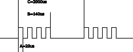
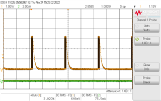
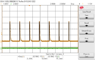
I need to generate PWM in chanel 2 and 3 as shown in Figure.
I am setting PWM frequency to 20 us .PWMa and PWM b need to be complementary The B and C timing is made using timer module as in code.
There are two problems.
a. When I am disabling the PWM, I need both A and B channel to pull low. However this is not happening.
b. Is there a better way to implement the above logic.
The following is the code.
#include "DSP28x_Project.h" // Device Headerfile and Examples Include File
// Prototype statements for functions found within this file.
void InitEPwm1Example(void);
interrupt void epwm1_isr(void);
interrupt void cpu_timer0_isr(void);
interrupt void epwm2_isr(void);
interrupt void epwm3_isr(void);
Uint32 DISCHARGE_PERIOD=2000;
Uint32 DISCHARGE_DUTY=140;
Uint32 count_discharge_period=1;
Uint32 count_discharge_duty=1;
void main(void)
{
// Step 1. Initialize System Control:
// PLL, WatchDog, enable Peripheral Clocks
// This example function is found in the DSP2802x_SysCtrl.c file.
InitSysCtrl();
// Step 2. Initalize GPIO:
// This example function is found in the DSP2802x_Gpio.c file and
// illustrates how to set the GPIO to it's default state.
// InitGpio(); // Skipped for this example
// For this case just init GPIO pins for ePWM1, ePWM2, ePWM3
// These functions are in the DSP2802x_EPwm.c file
InitEPwm1Gpio();
InitEPwm2Gpio();
InitEPwm3Gpio();
// Step 3. Clear all interrupts and initialize PIE vector table:
// Disable CPU interrupts
DINT;
// Initialize the PIE control registers to their default state.
// The default state is all PIE interrupts disabled and flags
// are cleared.
// This function is found in the DSP2802x_PieCtrl.c file.
InitPieCtrl();
InitCpuTimers(); // For this example, only initialize the Cpu Timers
// Disable CPU interrupts and clear all CPU interrupt flags:
IER = 0x0000;
IFR = 0x0000;
// Initialize the PIE vector table with pointers to the shell Interrupt
// Service Routines (ISR).
// This will populate the entire table, even if the interrupt
// is not used in this example. This is useful for debug purposes.
// The shell ISR routines are found in DSP2802x_DefaultIsr.c.
// This function is found in DSP2802x_PieVect.c.
InitPieVectTable();
// Interrupts that are used in this example are re-mapped to
// ISR functions found within this file.
EALLOW; // This is needed to write to EALLOW protected registers
PieVectTable.EPWM1_INT = &epwm1_isr;
PieVectTable.EPWM2_INT = &epwm2_isr;
PieVectTable.EPWM3_INT = &epwm3_isr;
EDIS; // This is needed to disable write to EALLOW protected registers
// Interrupts that are used in this example are re-mapped to
// ISR functions found within this file.
EALLOW; // This is needed to write to EALLOW protected registers
PieVectTable.TINT0 = &cpu_timer0_isr;
EDIS; // This is needed to disable write to EALLOW protected registers
// Step 4. Initialize the Device Peripheral. This function can be
// found in DSP2802x_CpuTimers.c
#if (CPU_FRQ_60MHZ)
// Configure CPU-Timer 0, 1, and 2 to interrupt every second:
// 60MHz CPU Freq, 1 second Period (in uSeconds)
ConfigCpuTimer(&CpuTimer0, 60, 1);
#endif
// Step 4. Initialize all the Device Peripherals:
// This function is found in DSP2802x_InitPeripherals.c
// InitPeripherals(); // Not required for this example
EALLOW;
SysCtrlRegs.PCLKCR0.bit.TBCLKSYNC = 0;
EDIS;
InitEPwm1Example();
EALLOW;
SysCtrlRegs.PCLKCR0.bit.TBCLKSYNC = 1;
EDIS;
// Enable CPU INT3 which is connected to EPWM1-3 INT:
// IER |= M_INT3;
// Enable CPU int1 which is connected to CPU-Timer 0,
IER |= M_INT1;
// Enable TINT0 in the PIE: Group 1 interrupt 7
PieCtrlRegs.PIEIER1.bit.INTx7 = 1;
// Enable EPWM INTn in the PIE: Group 3 interrupt 1-3
PieCtrlRegs.PIEIER3.bit.INTx1 = 1;
PieCtrlRegs.PIEIER3.bit.INTx2 = 1;
PieCtrlRegs.PIEIER3.bit.INTx3 = 1;
// Enable global Interrupts and higher priority real-time debug events:
EINT; // Enable Global interrupt INTM
ERTM; // Enable Global realtime interrupt DBGM
// To ensure precise timing, use write-only instructions to write to the entire register. Therefore, if any
// of the configuration bits are changed in ConfigCpuTimer and InitCpuTimers (in DSP2802x_CpuTimers.h), the
// below settings must also be updated.
CpuTimer0Regs.TCR.all = 0x4001; // Use write-only instruction to set TSS bit = 0
// Step 5. User specific code, enable interrupts:
// Enable global Interrupts and higher priority real-time debug events:
EINT; // Enable Global interrupt INTM
ERTM; // Enable Global realtime interrupt DBGM
// Step 6. IDLE loop. Just sit and loop forever (optional):
for(;;)
{
asm(" NOP");
}
}
interrupt void epwm1_isr(void)
{
EPwm1Regs.ETCLR.bit.INT = 1;
// Acknowledge this interrupt to receive more interrupts from group 3
PieCtrlRegs.PIEACK.all = PIEACK_GROUP3;
}
interrupt void epwm2_isr(void)
{
EPwm2Regs.ETCLR.bit.INT = 1;
// Acknowledge this interrupt to receive more interrupts from group 3
PieCtrlRegs.PIEACK.all = PIEACK_GROUP3;
}
interrupt void epwm3_isr(void)
{
EPwm3Regs.ETCLR.bit.INT = 1;
// Acknowledge this interrupt to receive more interrupts from group 3
PieCtrlRegs.PIEACK.all = PIEACK_GROUP3;
}
interrupt void cpu_timer0_isr(void)
{
if (count_discharge_duty<DISCHARGE_DUTY && count_discharge_period<=DISCHARGE_PERIOD)
{
count_discharge_duty=count_discharge_duty+1;
count_discharge_period=count_discharge_period+1;
}
else if (count_discharge_duty>=DISCHARGE_DUTY && count_discharge_period<DISCHARGE_PERIOD)
{
count_discharge_period=count_discharge_period+1;
EPwm3Regs.TBCTR = 0x0000;
EPwm2Regs.TBCTR = 0x0000;
}
else if (count_discharge_duty== DISCHARGE_DUTY && count_discharge_period==DISCHARGE_PERIOD)
{
count_discharge_duty=1;
count_discharge_period=1;
EPwm3Regs.AQCTLA.bit.PRD = AQ_SET;
EPwm3Regs.AQCTLA.bit.CAU = AQ_CLEAR;
EPwm3Regs.AQCTLB.bit.PRD= AQ_CLEAR;
EPwm3Regs.AQCTLB.bit.CAU = AQ_SET;
EPwm2Regs.AQCTLA.bit.PRD = AQ_SET;
EPwm2Regs.AQCTLA.bit.CAU = AQ_CLEAR;
EPwm2Regs.AQCTLB.bit.PRD = AQ_CLEAR;
EPwm2Regs.AQCTLB.bit.CAU = AQ_SET;
}
// CpuTimer0.InterruptCount++;
// Acknowledge this interrupt to receive more interrupts from group 1
PieCtrlRegs.PIEACK.all = PIEACK_GROUP1;
}
void InitEPwm1Example()
{
// EPWM Module 1 config
EPwm1Regs.TBPRD = 500; // Period = 1201 TBCLK counts
EPwm1Regs.TBPHS.half.TBPHS = 0; // Set Phase register to zero
EPwm1Regs.TBCTL.bit.CTRMODE = TB_COUNT_UP; // Asymmetrical mode
EPwm1Regs.TBCTL.bit.PHSEN = TB_DISABLE; // Phase loading disabled
EPwm1Regs.TBCTL.bit.PRDLD = TB_SHADOW;
EPwm1Regs.TBCTL.bit.SYNCOSEL = TB_SYNC_DISABLE;
EPwm1Regs.TBCTL.bit.HSPCLKDIV = TB_DIV1; // TBCLK = SYSCLKOUT // if this is not includede int the code the default frequency becomes half
EPwm1Regs.TBCTL.bit.CLKDIV = TB_DIV1;
EPwm1Regs.CMPCTL.bit.SHDWAMODE = CC_SHADOW;
EPwm1Regs.CMPCTL.bit.SHDWBMODE = CC_SHADOW;
EPwm1Regs.CMPCTL.bit.LOADAMODE = CC_CTR_ZERO; // load on CTR=Zero
EPwm1Regs.CMPCTL.bit.LOADBMODE = CC_CTR_ZERO; // load on CTR=Zero
EPwm1Regs.AQCTLA.bit.PRD = AQ_SET;
EPwm1Regs.AQCTLA.bit.CAU = AQ_CLEAR;
EPwm1Regs.AQCTLB.bit.PRD = AQ_CLEAR;
EPwm1Regs.AQCTLB.bit.CAU = AQ_SET;
EPwm1Regs.CMPA.half.CMPA = 250;
// Active Low PWMs - Setup Deadband
EPwm1Regs.DBCTL.bit.OUT_MODE = DB_FULL_ENABLE;
EPwm1Regs.DBCTL.bit.POLSEL = DB_ACTV_HIC;
//EPwm1Regs.DBCTL.bit.IN_MODE = DBA_ALL;
EPwm1Regs.DBRED = 20;
EPwm1Regs.DBFED = 20;
//EPwm1_DB_Direction = DB_UP;
// Interrupt where we will change the Deadband
EPwm1Regs.ETSEL.bit.INTSEL = ET_CTR_ZERO; // Select INT on Zero event
EPwm1Regs.ETSEL.bit.INTEN = 1; // Enable INT
EPwm1Regs.ETPS.bit.INTPRD = ET_3RD; // Generate INT on 3rd event
// EPWM2 Configuration
EPwm2Regs.TBPRD = 1200; // Period = 1201 TBCLK counts
EPwm2Regs.TBPHS.half.TBPHS = 0; // Set Phase register to zero
EPwm2Regs.TBCTL.bit.CTRMODE = TB_COUNT_UP; // Asymmetrical mode
EPwm2Regs.TBCTL.bit.PHSEN = TB_DISABLE; // Phase loading disabled
EPwm2Regs.TBCTL.bit.PRDLD = TB_SHADOW;
EPwm2Regs.TBCTL.bit.SYNCOSEL = TB_SYNC_DISABLE;
EPwm2Regs.TBCTL.bit.HSPCLKDIV = TB_DIV1; // TBCLK = SYSCLKOUT // if this is not includede int the code the default frequency becomes half
EPwm2Regs.TBCTL.bit.CLKDIV = TB_DIV1;
EPwm2Regs.CMPCTL.bit.SHDWAMODE = CC_SHADOW;
EPwm2Regs.CMPCTL.bit.SHDWBMODE = CC_SHADOW;
EPwm2Regs.CMPCTL.bit.LOADAMODE = CC_CTR_ZERO; // load on CTR=Zero
EPwm2Regs.CMPCTL.bit.LOADBMODE = CC_CTR_ZERO; // load on CTR=Zero
EPwm2Regs.AQCTLA.bit.PRD = AQ_SET;
EPwm2Regs.AQCTLA.bit.CAU = AQ_CLEAR;
EPwm2Regs.AQCTLB.bit.PRD = AQ_CLEAR;
EPwm2Regs.AQCTLB.bit.CAU = AQ_SET;
EPwm2Regs.CMPA.half.CMPA = 600;
// Active Low PWMs - Setup Deadband
EPwm2Regs.DBCTL.bit.OUT_MODE = DB_FULL_ENABLE;
EPwm2Regs.DBCTL.bit.POLSEL = DB_ACTV_HIC;
//EPwm1Regs.DBCTL.bit.IN_MODE = DBA_ALL;
EPwm2Regs.DBRED = 20;
EPwm2Regs.DBFED = 20;
//EPwm1_DB_Direction = DB_UP;
// // Interrupt where we will change the Deadband
// EPwm2Regs.ETSEL.bit.INTSEL = ET_CTR_ZERO; // Select INT on Zero event
// EPwm2Regs.ETSEL.bit.INTEN = 1; // Enable INT
// EPwm2Regs.ETPS.bit.INTPRD = ET_3RD; // Generate INT on 3rd event
// EPWM3 Configuration
EPwm3Regs.TBPRD = 1200; // Period = 1201 TBCLK counts
EPwm3Regs.TBPHS.half.TBPHS = 0; // Set Phase register to zero
EPwm3Regs.TBCTL.bit.CTRMODE = TB_COUNT_UP; // Asymmetrical mode
EPwm3Regs.TBCTL.bit.PHSEN = TB_DISABLE; // Phase loading disabled
EPwm3Regs.TBCTL.bit.PRDLD = TB_SHADOW;
EPwm3Regs.TBCTL.bit.SYNCOSEL = TB_SYNC_DISABLE;
EPwm3Regs.TBCTL.bit.HSPCLKDIV = TB_DIV1; // TBCLK = SYSCLKOUT // if this is not includede int the code the default frequency becomes half
EPwm3Regs.TBCTL.bit.CLKDIV = TB_DIV1;
EPwm3Regs.CMPCTL.bit.SHDWAMODE = CC_SHADOW;
EPwm3Regs.CMPCTL.bit.SHDWBMODE = CC_SHADOW;
EPwm3Regs.CMPCTL.bit.LOADAMODE = CC_CTR_ZERO; // load on CTR=Zero
EPwm3Regs.CMPCTL.bit.LOADBMODE = CC_CTR_ZERO; // load on CTR=Zero
EPwm3Regs.AQCTLA.bit.PRD= AQ_SET;
EPwm3Regs.AQCTLA.bit.CAU = AQ_CLEAR;
EPwm3Regs.AQCTLB.bit.PRD = AQ_CLEAR;
EPwm3Regs.AQCTLB.bit.CAU = AQ_SET;
EPwm3Regs.CMPA.half.CMPA = 600;
// Active Low PWMs - Setup Deadband
EPwm3Regs.DBCTL.bit.OUT_MODE = DB_FULL_ENABLE;
EPwm3Regs.DBCTL.bit.POLSEL = DB_ACTV_HIC;
//EPwm1Regs.DBCTL.bit.IN_MODE = DBA_ALL;
EPwm3Regs.DBRED = 20;
EPwm3Regs.DBFED = 20;
//EPwm1_DB_Direction = DB_UP;
// Interrupt where we will change the Deadband
EPwm3Regs.ETSEL.bit.INTSEL = ET_CTR_ZERO; // Select INT on Zero event
EPwm3Regs.ETSEL.bit.INTEN = 1; // Enable INT
EPwm3Regs.ETPS.bit.INTPRD = ET_3RD; // Generate INT on 3rd event
// Enable TZ1 and TZ2 as one cycle-by-cycle trip sources
EALLOW;
EPwm2Regs.TZFRC.bit.CBC = 1;
EPwm2Regs.TZCTL.bit.TZA = TZ_FORCE_LO;
EPwm2Regs.TZCTL.bit.TZB = TZ_FORCE_LO;
EPwm3Regs.TZFRC.bit.CBC = 1;
EPwm3Regs.TZCTL.bit.TZA = TZ_FORCE_LO;
EPwm3Regs.TZCTL.bit.TZB = TZ_FORCE_LO;
EDIS;
}
//===========================================================================
// No more.
//===========================================================================