Part Number: TMS320F28386S
Other Parts Discussed in Thread: HALCOGEN
It was necessary for me to emulate SCI_Boot as our hardware was not configured properly and the board will not be respun.
I got my pseudo SCI_boot to run and it accepted 23300+ bytes from the serial flash programmer. The initial destination is 0 and it correctly builds up from there. However, I am not sure it is safe to write to this starting location but I cannot tell for sure from the linker cmd file. Also if I interpret correctly the stack is at RAMM0_1 so that is being overwritten.
So I see 3 alternatives:
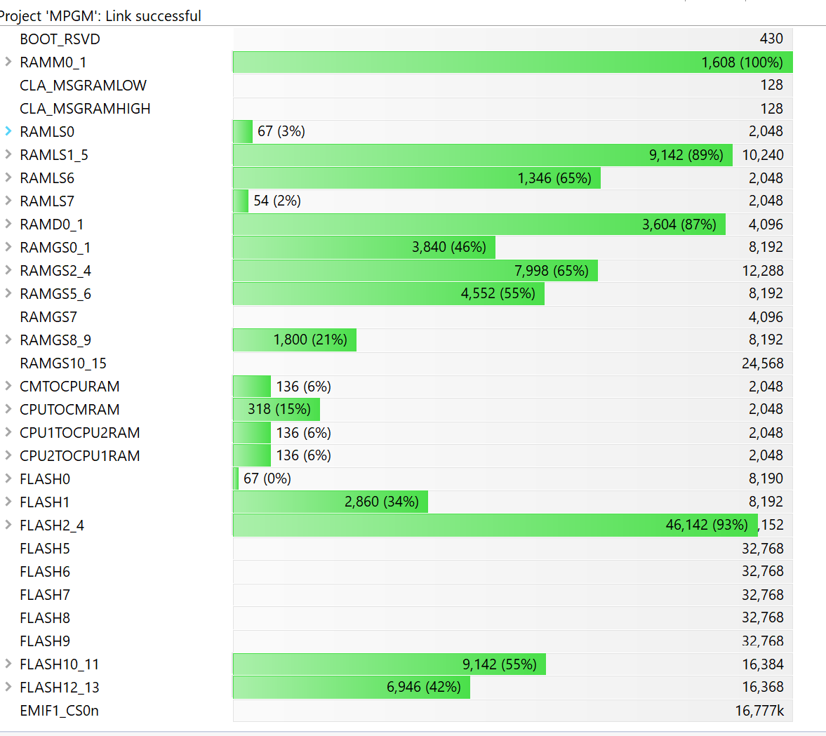
1) Adjust the linker command file so that 24K of spaces is skipped which seems would take up memory into GS1. Which may not leave enough for the app. A memory allocation map for our regular app is below.
2) Modify my pseudo SCI boot program to use an offset to load to our external RAM at 0x80000000, 16Mx16, IS45S16160J-7TLA2. I am not sure about the the first 2 blocks as the first one is destined for address 0 and the next for 0x1B4 which is in RAMM0 which starts at 0x1B1Hey
3) Knuckle down and figure out how to put the flash kernel into flash permanently. If I do so, to run it from our main app would I load a function pointer with that flash address? Would the stack and any other addresses need to be changed?
My choice is number three as there seems to be plenty of flash available. But the repo flash_kernel_c28x_dual_ex1_c28x1 is naturally RAM based and I am having problems converting it to flash based. I would appreciate your observations and advise.
This is our current linker file:
#if 1
MEMORY
{

   BOOT_RSVD        : origin = 0x000002, length = 0x0001AE     /* Part of M0, BOOT rom will use this for stack */
   RAMM0_1          : origin = 0x0001B0, length = 0x000648
   // RAMM1_RSVD       : origin = 0x0007F8, length = 0x000008         /* Reserve and do not use for code as per the errata advisory "Memory: Prefetching Beyond Valid Memory" */
   CLA_MSGRAMLOW    : origin = 0x001480, length = 0x000080
   CLA_MSGRAMHIGH   : origin = 0x001500, length = 0x000080
   RAMD0_1          : origin = 0x00C000, length = 0x001000
   RAMLS0           : origin = 0x008000, length = 0x000800
   RAMLS1_5         : origin = 0x008800, length = 0x002800
   RAMLS6           : origin = 0x00B000, length = 0x000800
   RAMLS7           : origin = 0x00B800, length = 0x000800
   RAMGS0_1         : origin = 0x00D000, length = 0x002000
   RAMGS2_4         : origin = 0x00F000, length = 0x003000
   RAMGS5_6         : origin = 0x012000, length = 0x002000
   RAMGS7           : origin = 0x014000, length = 0x001000
   RAMGS8_9         : origin = 0x015000, length = 0x002000
   RAMGS10_15       : origin = 0x017000, length = 0x005FF8
   // RAMGS15_RSVD     : origin = 0x01CFF8, length = 0x000008         /* Reserve and do not use for code as per the errata advisory "Memory: Prefetching Beyond Valid Memory" */

#ifdef __TI_COMPILER_VERSION__
   #if __TI_COMPILER_VERSION__ >= 20012000
GROUP {      /* GROUP memory ranges for crc/checksum of entire flash */
   #endif
#endif
   /* BEGIN is used for the "boot to Flash" bootloader mode   */
   BEGIN            : origin = 0x080000, length = 0x000002
   /* Flash sectors */
   FLASH0           : origin = 0x080002, length = 0x001FFE  /* on-chip Flash */
   FLASH1           : origin = 0x082000, length = 0x002000  /* on-chip Flash */
   FLASH2_4         : origin = 0x084000, length = 0x00C000  /* on-chip Flash */
   FLASH5           : origin = 0x090000, length = 0x008000  /* on-chip Flash */
   FLASH6           : origin = 0x098000, length = 0x008000  /* on-chip Flash */
   FLASH7           : origin = 0x0A0000, length = 0x008000  /* on-chip Flash */
   FLASH8           : origin = 0x0A8000, length = 0x008000  /* on-chip Flash */
   FLASH9           : origin = 0x0B0000, length = 0x008000  /* on-chip Flash */
   FLASH10_11       : origin = 0x0B8000, length = 0x004000  /* on-chip Flash */
   FLASH12_13       : origin = 0x0BC000, length = 0x003FF0  /* on-chip Flash */
   // FLASH13_RSVD     : origin = 0x0BFFF0, length = 0x000010    /* Reserve and do not use for code as per the errata advisory "Memory: Prefetching Beyond Valid Memory" */
#ifdef __TI_COMPILER_VERSION__
  #if __TI_COMPILER_VERSION__ >= 20012000
}  crc(_table_name, algorithm=C28_CHECKSUM_16)
  #endif
#endif

   CPUTOCMRAM      : origin = 0x039000, length = 0x000800
   CMTOCPURAM      : origin = 0x038000, length = 0x000800
   CPU1TOCPU2RAM   : origin = 0x03A000, length = 0x000800
   CPU2TOCPU1RAM   : origin = 0x03B000, length = 0x000800

   RESET            : origin = 0x3FFFC0, length = 0x000002

   EMIF1_CS0n      : origin = 0x80000000, length = 0x01000000
}

SECTIONS
{
   codestart           : > BEGIN, ALIGN(4)
   .text               : > FLASH2_4, ALIGN(4)
   .cinit              : > FLASH1, ALIGN(4)
   .switch             : > FLASH1, ALIGN(4)
   .reset              : > RESET, TYPE = DSECT /* not used, */
   .stack              : > RAMM0_1

#if defined(__TI_EABI__)
   .init_array      : > FLASH1, ALIGN(4)
   .bss             : > RAMGS2_4
   .bss:output      : > RAMGS2_4
   .bss:cio         : > RAMGS2_4
   .data            : > RAMGS5_6
   .sysmem          : > RAMGS2_4
   /* Initalized sections go in Flash */
   .const           : > FLASH12_13, ALIGN(4)
#else
   .pinit           : > FLASH1, ALIGN(4)
   .ebss            : > RAMGS2_4
   .esysmem         : > RAMGS2_4
   .cio             : > RAMGS2_4
   /* Initalized sections go in Flash */
   .econst          : >> FLASH12_13, ALIGN(4)
#endif

   .farbss          : > EMIF1_CS0n
   .farconst        : > EMIF1_CS0n
   .em1_cs0         : > EMIF1_CS0n

/*** CLA Compiler Required Sections ***/
   .scratchpad         : > RAMLS7                /* Scratchpad memory for the CLA C Compiler */
   .const_cla          : > RAMLS7

   ramgs0 : > RAMGS0_1, type=NOINIT

   MSGRAM_CPU1_TO_CPU2 : > CPU1TOCPU2RAM, type=NOINIT
   MSGRAM_CPU2_TO_CPU1 : > CPU2TOCPU1RAM, type=NOINIT
   MSGRAM_CPU_TO_CM    : > CPUTOCMRAM, type=NOINIT
   MSGRAM_CM_TO_CPU    : > CMTOCPURAM, type=NOINIT

   #if defined(__TI_EABI__)
       .TI.ramfunc : {} LOAD = FLASH0,
                        RUN = RAMLS0,
                        LOAD_START(RamfuncsLoadStart),
                        LOAD_SIZE(RamfuncsLoadSize),
                        LOAD_END(RamfuncsLoadEnd),
                        RUN_START(RamfuncsRunStart),
                        RUN_SIZE(RamfuncsRunSize),
                        RUN_END(RamfuncsRunEnd),
                        ALIGN(4)
    #else
       .TI.ramfunc : {} LOAD = FLASH0,
                        RUN = RAMLS0,
                        LOAD_START(_RamfuncsLoadStart),
                        LOAD_SIZE(_RamfuncsLoadSize),
                        LOAD_END(_RamfuncsLoadEnd),
                        RUN_START(_RamfuncsRunStart),
                        RUN_SIZE(_RamfuncsRunSize),
                        RUN_END(_RamfuncsRunEnd),
                        ALIGN(4)
    #endif

   DataBufferSection   : > RAMGS7, ALIGN(4)
   LogSection          : > RAMD0_1, ALIGN(4)
   ParamSection        : > RAMGS8_9, ALIGN(4)
   ClaToCpuMsgRAM      : > CLA_MSGRAMLOW              /* Link to CLA Message RAM */
   CpuToClaMsgRAM      : > CLA_MSGRAMHIGH             /* Link to CLA Message RAM */
   ClaData             : > RAMLS6                     /* Link to CLA Data RAM */
   .bss_cla            : > RAMLS6                     /* Link to CLA Data RAM */

   /* Link to CLA Program RAM */
   Cla1Prog            : LOAD = FLASH10_11,
                         RUN = RAMLS1_5,
                         LOAD_START(ClaProgLoadStart),
                         RUN_START(ClaProgRunStart),
                         LOAD_SIZE(ClaProgLoadSize) ,
                         ALIGN(4)

   /* crc/checksum section configured as COPY section to avoid including in executable */
   .TI.memcrc          : type = COPY

}
Here is the current memory allocation.