This thread has been locked.

If you have a related question, please click the "Ask a related question" button in the top right corner. The newly created question will be automatically linked to this question.

TMS320F28035: Compensation Designer GUI

Part Number: TMS320F28035
Other Parts Discussed in Thread: SFRA

Hi Team,

Here're some issues from the customer may need your help:

The customer is currently working on the routine for BuckBoostBiDir_F2803x. After the actual programming test, it is found that if the output voltage is set too high at the beginning, there will be no output.

It is speculated that it was caused by excessive compensation that exceeded the upper limit of DUTY at the beginning. So the customer wants to study how the 3p3z compensation coefficient is set in the program.

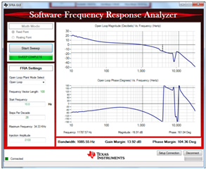
The customer has several questions about the operation of c2000 Compensation Designer:

1. Is control Freq switching the frequency Fsw? In this example, Fsw is 250kHz, so control Freq is 250kHz, right?

2. What does Plant mean in the three curves? This routine is a feedback circuit. Why need to measure the open loop (OL) curve? How is the compensation curve (Comp) considered a good compensation?

3. There are KDC, fz0, fz1, fz2, fp0, fp1, fp2 and other parameters in 3p3z, how to set these parameters?

--

Thanks & Regards

Yale

  • 1. Is control Freq switching the frequency Fsw? In this example, Fsw is 250kHz, so control Freq is 250kHz, right?

    The control frequency is 83kHz (250KHz/3). This is mentioned in the user guide.

    2. What does Plant mean in the three curves? This routine is a feedback circuit. Why need to measure the open loop (OL) curve? How is the compensation curve (Comp) considered a good compensation?

    Plant means the system response in open-loop, i.e. with the compensator bypassed. You should configure the code to run in open-loop, manually adjust the duty cycle to reach the desired VOUT, and run SFRA to collect the system response. Once you have the plant data, you can upload to the compensation designer and tune using the DC gain and pole/zero locations.

    #define OPEN_LOOP 0 // write 0 for closed loop operation

    3. There are KDC, fz0, fz1, fz2, fp0, fp1, fp2 and other parameters in 3p3z, how to set these parameters?

    You need to adjust these parameters to get the desired OL response, i.e. bandwidth, phase margin, and gain margin. Once you have the coefficients you need, you can copy them to the code, build it in closed-loop, then run SFRA again to verify if the system response matches your desired output.

  • You need to adjust these parameters to get the desired OL response, i.e. bandwidth, phase margin, and gain margin. Once you have the coefficients you need, you can copy them to the code, build it in closed-loop, then run SFRA again to verify if the system response matches your desired output.

    The customer is currently working on the routine for the BuckBoostBiDir_F2803x. The Bode plot he measured using SFRA is completely different from the one measured by USER GUIDE.

    USERGUIDE:

    His:

    Moreover, the result obtained by using SFRA to scan once again under the same input and output voltage (Vin 50V/ Vout 40V) is different from the result of the first scan:

    He tried to use the compensation designer to compensate the waveform detected by SFRA, and it showed a stable loop, but no matter how the output voltage was set, he could not reach the set value, and it stopped when it rose slowly to 2V:

    Why is this so?

    --

    Thanks & Regards

    Yale

  • Hello Yale,

    I think this is related to this post:

    https://e2e.ti.com/support/microcontrollers/c2000-microcontrollers-group/c2000/f/c2000-microcontrollers-forum/1196560/tms320f28035-buckboostdir_f2803x

    If so, the code is running on a custom board. There are issues on that board that have not been resolved yet. Before moving to a stable SFRA scan, we need to resolve those issues first.