- Ask a related questionWhat is a related question?A related question is a question created from another question. When the related question is created, it will be automatically linked to the original question.
This thread has been locked.
If you have a related question, please click the "Ask a related question" button in the top right corner. The newly created question will be automatically linked to this question.
Hello,
I am working on setting up the WD and I noticed the reset time value using a scope plugged on the XRSn pin is not what I expected.
After enabling the WD with a presale of 1 (WDPS = 0, WDCLK = INTOSC1/512/1), I am expecting to have a time between each continuous WD reset around 13.1ms with INTOSC1 = 10 MHz.
1/(10MHz/512) * 256 (WDCR) = 13.1ms.
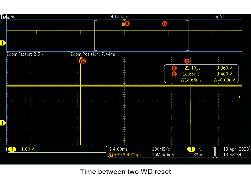
I measure around 19ms (see below):
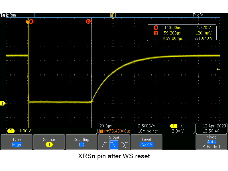
Then, when I measure the time of the XRSn, I am expecting to get 512 x INTOSC1 = 51.2us (per the datasheet) but I measure around 60us (see below):
Does anyone know what is going on?
Thank you.
Laurent
Hi Laurent,
After enabling the WD with a presale of 1 (WDPS = 0, WDCLK = INTOSC1/512/1), I am expecting to have a time between each continuous WD reset around 13.1ms with INTOSC1 = 10 MHz.
1/(10MHz/512) * 256 (WDCR) = 13.1ms.
I measure around 19ms (see below):
after reset device runs though the BOOTROM and cinit function and then runs the application code. BOOTROM and cinit takes significant amount of time hence you see big number.
Then, when I measure the time of the XRSn, I am expecting to get 512 x INTOSC1 = 51.2us (per the datasheet) but I measure around 60us (see below):
How are you measuring this ? XRSn has a pull-up and that will cause some delay from 1 -> 0 transition hence you'll see a bigger pulse than 51.2us. This looks ok to me.
Regards,
Vivek Singh
Thank you Vivek,
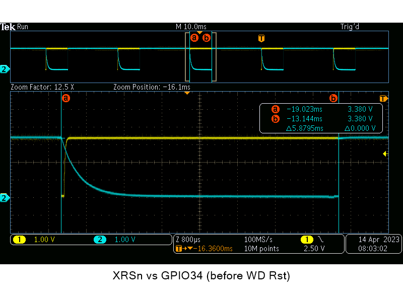
I was able to confirm the delay it takes from the time of the reset (scope connected to XRSn, yellow line) all the way to the execution before WD reset (scope connected to GPIO34 output, blue line). Your were right it takes about 6 ms:
Regarding the reset time of XRSn, I have the TMDSCNCD28379D_v1_0 Control Card with the docking station. I measure the signal with a scope on pin 120 of the docking station:

Could you please explain to me why a pull-up would delay the signal by 8us? Sorry I don't get your point.
Thank you
Laurent
Laurent,
RC circuit will delay the rise and fall time of signal and extend the duration reset pulse. Do you see any major concern you see with 8us additional delay ?
Regards,
Vivek Singh
No, no major concern, I just need to explain and document every detail design in case of an audit.
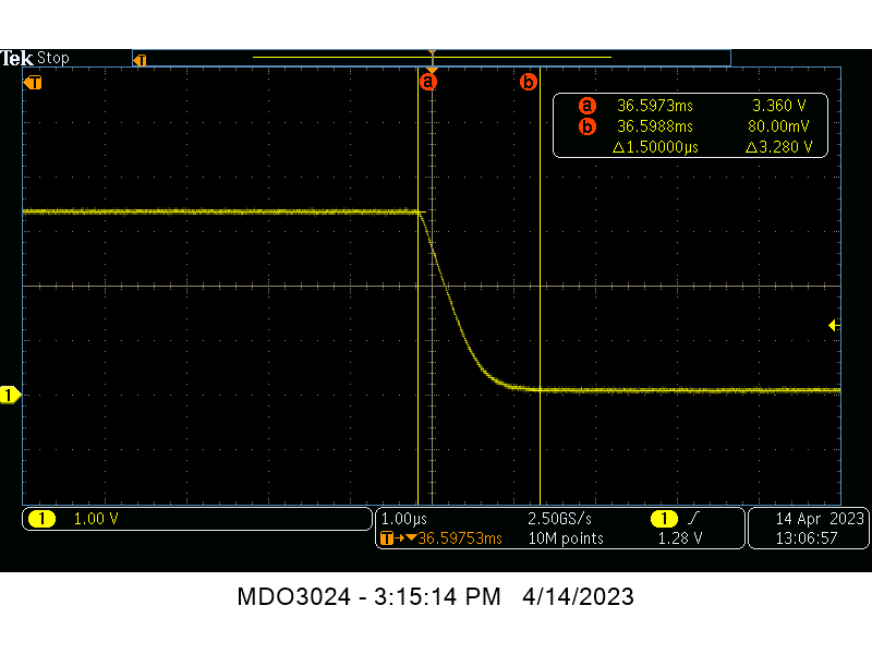
I see a slight delay but not 8us more around 1.5us.
Lauernt,
This is with the INTOSC2, which may not be running at exactly10 MHz. Can you meaure the exact frequency of INTOSC?
Isn't the WD source clock INTOSC1?

I redirected INTOSC1 to XCLKOUT in order to measure the frequency, it seems to be right at 10MHz, however I quite don't understand why I do not observe straight edges. XCLKOUT is rated at 50MHz max. I am using TMDSCNCD28379D_v1_0 Control Card with the docking station and I don't see any RC circuitry on pin GPIO73. I calibrated my probe to measure straight edges.
It baffles me!
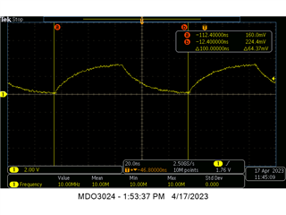
Any thoughts?
Yes, WD is sourced from INTOSC1 but the point Hareesh was making is that during reset trim values also gets reset hence INTOSC will have some variation. What you are observing on clock is after reset is released and with proper trim value.
Regards,
Vivek Singh
Okay, that makes sense. I will go with this explanation.
Thank you very much.
Laurent