Other Parts Discussed in Thread: LAUNCHXL-F280039C, SYSCONFIG, LAUNCHXL-F280049C, C2000WARE
Hey,
I am facing some problems in implementing active-high complementary PWM with dead-band and high resolution mode on TMS320F280039C. I want to use it to control a three-phase six-switch inverter with symmetrical PWM pattern or space vector modulation.
At first, everthying looks good. But by varying the duty cycle across the full range, I've detected glitches on the rising edges, as you can see on my following measurements:
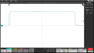
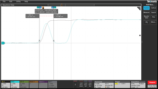
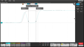
CH1 (black): PWM2A output, J4 pin 38
CH2 (blue): PWM1A output, J4 pin 40
I have written small test code for use on the LAUNCHXL-F280039C with fixed duty cylces which shows the glitches from my measurements:
#include "f28x_project.h"
#include "sfo_v8.h"

#define RED_FED 42                      // t_red = t_fed = RED_FED * t_pwmclk = 42 / 120 MHz = ca. 350 ns

void init_pwm_gpio(void);
void init_pwm(void);
void update_epwm1(float dc);

volatile struct EPWM_REGS *ePWM[3] = {0, &EPwm1Regs, &EPwm2Regs};

Uint16 status = SFO_INCOMPLETE;
int MEP_ScaleFactor = 0; //scale factor value

//
// Main
//
void main(void)
{
    //
    // Initialize device clock and peripherals
    //
    InitSysCtrl();

    //
    // Initialize GPIO
    //
    InitGpio();

    //
    // Disable CPU interrupts
    //
    DINT;

    //
    // Initialize the PIE control registers to their default state.
    // The default state is all PIE interrupts disabled and flags
    // are cleared.
    //
    InitPieCtrl();

    //
    // Disable CPU interrupts and clear all CPU interrupt flags:
    //
    IER = 0x0000;
    IFR = 0x0000;

    //
    // Initialize the PIE vector table with pointers to the shell Interrupt
    // Service Routines (ISR).
    //
    InitPieVectTable();

    init_pwm_gpio();
    init_pwm();

    EPwm2Regs.CMPA.bit.CMPA = 560;
    EPwm2Regs.CMPA.bit.CMPAHR = 0;
    EPwm2Regs.CMPB.bit.CMPBHR = 0;

    update_epwm1(0.867F);

    EINT;           // Enable Global interrupt INTM
    ERTM;           // Enable Global realtime interrupt DBGM

    while(1)
    {
    }
}

void update_epwm1(float dc)
{
    uint16_t cmpa = 0;
    uint32_t cmpa_hr_temp = 0;
    uint16_t cmpa_hr = 0;

    cmpa = (uint16_t)((dc * 300) + 300);

    // Duty Cycle Range Limitation in high resolution period mode
    // which includes the up-down count mode with MEP on both rising edge and falling edge.
    // MEP is inactive in TBCTR range [0, 3[ and ]PFC_PERIOD - 3, PFC_PERIOD]
    if((cmpa >= 3) && (cmpa <= (600 - 3)))
    {
        cmpa_hr_temp = (uint32_t)((dc * ((long)(300) << 16)) + (300  << 16));
        cmpa_hr = cmpa_hr_temp - ((long)(cmpa) << 16);
    }
    else
    {
        if(cmpa < 3)
        {
            cmpa = 0;
        }
        else
        {
            cmpa = 600;
        }
        cmpa_hr = 0;
    }

    EPwm1Regs.CMPA.bit.CMPA = cmpa;
    EPwm1Regs.CMPA.bit.CMPAHR = cmpa_hr;
    EPwm1Regs.CMPB.bit.CMPBHR = cmpa_hr;
}

void init_pwm_gpio(void)
{
    EALLOW;
    GpioCtrlRegs.GPAPUD.bit.GPIO0 = 1;      // Disable pull-up on GPIO0 (EPWM1A)
    GpioCtrlRegs.GPAPUD.bit.GPIO1 = 1;      // Disable pull-up on GPIO1 (EPWM1B)

    GpioCtrlRegs.GPAPUD.bit.GPIO2 = 1;      // Disable pull-up on GPIO2 (EPWM2A)
    GpioCtrlRegs.GPAPUD.bit.GPIO3 = 1;      // Disable pull-up on GPIO3 (EPWM2B)

    GpioCtrlRegs.GPAMUX1.bit.GPIO0 = 1;     // Configure GPIO0 as EPWM1A
    GpioCtrlRegs.GPAMUX1.bit.GPIO1 = 1;     // Configure GPIO1 as EPWM1B

    GpioCtrlRegs.GPAMUX1.bit.GPIO2 = 1;     // Configure GPIO2 as EPWM2A
    GpioCtrlRegs.GPAMUX1.bit.GPIO3 = 1;     // Configure GPIO3 as EPWM2B

    GpioCtrlRegs.GPALOCK.bit.GPIO0 = 1;     // lock GPIO0 configuration
    GpioCtrlRegs.GPALOCK.bit.GPIO1 = 1;     // lock GPIO1 configuration

    GpioCtrlRegs.GPALOCK.bit.GPIO2 = 1;     // lock GPIO2 configuration
    GpioCtrlRegs.GPALOCK.bit.GPIO3 = 1;     // lock GPIO3 configuration

    EDIS;
}

void init_pwm(void)
{

    uint16_t i;

    EALLOW;
    CpuSysRegs.PCLKCR0.bit.TBCLKSYNC = 0;       // Disable EPWM Time Base Clock gating
    EDIS;

    for(i = 1; i < 3; i++)
        {
            // Time-Base Submodule
            (*ePWM[i]).TBPRD = 600;                 // Set timer period
            (*ePWM[i]).TBPRDHR = 0;                 // HR Period

            (*ePWM[i]).TBCTR = 0x0000;              // Clear counter

            (*ePWM[i]).TBCTL.bit.PRDLD = 0;         // Active Period Reg Load from Shadow
            (*ePWM[i]).TBCTL.bit.CTRMODE = 2;       // Up-Down-Count mode
            (*ePWM[i]).TBCTL.bit.FREE_SOFT = 2;     // free run in emulation mode
            (*ePWM[i]).TBCTL.bit.PHSDIR = 1;        // Count up after the synchronization event
            (*ePWM[i]).TBCTL.bit.PHSEN = 0;         // Disable load event when an EPWMxSYNCI input signal occurs
            (*ePWM[i]).TBCTL.bit.HSPCLKDIV = 0;     // Clock ratio / 1
            (*ePWM[i]).TBCTL.bit.CLKDIV = 0;        // Clock ratio / 1

            // Synchronization in- and output
            (*ePWM[i]).EPWMSYNCINSEL.bit.SEL = 0;    // Disables all inputs for this module
            (*ePWM[i]).EPWMSYNCOUTEN.bit.SWEN = 0;   // Disable EPWMxSYNCO at SWFSYNC

            // Counter-Compare Submodule
            (*ePWM[i]).CMPCTL.bit.LOADAMODE = 0;     // Load CMPA when TBCTR = 0
            (*ePWM[i]).CMPCTL.bit.SHDWAMODE = 0;     // enable CMPA shadow mode
            (*ePWM[i]).CMPA.bit.CMPA = 300;           // Set default CMPA value

            // Action-Qualifier Submodule
            // ePWMxA on-time = (1200 - 2 * CMPA) * (1 / 120 MHz)
            // ePWMxB on-time = 2* CMPA  * (1 / 120 MHz)
            (*ePWM[i]).AQCTLA.bit.ZRO = 1;           // Clear ePWMxA when TBCTR = 0
            (*ePWM[i]).AQCTLA.bit.CAU = 2;           // Set ePWMxA when TBCTR = CMPA on up-count
            (*ePWM[i]).AQCTLA.bit.CAD = 1;           // Clear ePWMxA when TBCTR = CMPA on down-count


            (*ePWM[i]).DBCTL.bit.HALFCYCLE = 1;         // clock DB counters at half TBCLK rate
            (*ePWM[i]).DBCTL.bit.DEDB_MODE = 0;         // RED to Input A, FED to Input A
            (*ePWM[i]).DBCTL.bit.IN_MODE = 0;
            (*ePWM[i]).DBCTL.bit.OUT_MODE = 3;          // RED to A path, FED to B path
            (*ePWM[i]).DBCTL.bit.POLSEL = 2;            // B path inverted
            (*ePWM[i]).DBCTL.bit.OUTSWAP = 0;           // A path to OutA, B path to OutB
            (*ePWM[i]).DBCTL.bit.SHDWDBFEDMODE = 1;     // FED shandow load mode
            (*ePWM[i]).DBCTL.bit.SHDWDBREDMODE = 1;     // RED shandow load mode
            (*ePWM[i]).DBCTL.bit.LOADFEDMODE = 2;       // Load on TBCTR = 0 or TBCTR = PRD
            (*ePWM[i]).DBCTL.bit.LOADREDMODE = 2;       // Load on TBCTR = 0 or TBCTR = PRD

            (*ePWM[i]).DBRED.bit.DBRED = 2 * RED_FED;
            (*ePWM[i]).DBFED.bit.DBFED = 2 * RED_FED;

            EALLOW;
            (*ePWM[i]).HRCNFG.all = 0x0;
            (*ePWM[i]).HRCNFG.bit.EDGMODE = 3;          // MEP control of both edges
            (*ePWM[i]).HRCNFG.bit.CTLMODE = 0;          // Duty control mode
            (*ePWM[i]).HRCNFG.bit.HRLOAD = 2;           // Load CMPAHR when TBCTR = 0 or TBCTR = PRD
            (*ePWM[i]).HRCNFG.bit.AUTOCONV = 1;         // Automatic HRMSTEP scaling is enabled

            //
            // CMPBHR is used for duty-control with dead-band in up-down-count mode and must be set to same value as CMPA
            //
            (*ePWM[i]).HRCNFG.bit.EDGMODEB = 3;          // MEP control of both edges
            (*ePWM[i]).HRCNFG.bit.CTLMODEB = 0;          // Duty control mode
            (*ePWM[i]).HRCNFG.bit.HRLOADB = 2;           // Load CMPBHR when TBCTR = 0 or TBCTR = PRD
            //

            (*ePWM[i]).HRCNFG2.bit.EDGMODEDB = 3;       // MEP control of both edges (DBREDHR and DBFEDHR)
            (*ePWM[i]).HRCNFG2.bit.CTLMODEDBRED = 2;    // load shadow register when CTR = Zero or CTR = PRD
            (*ePWM[i]).HRCNFG2.bit.CTLMODEDBFED = 2;    // load shadow register when CTR = Zero or CTR = PRD

            (*ePWM[i]).HRPWR.bit.CALPWRON = 1;          // Enables MEP calibration logic

            (*ePWM[i]).HRPCTL.bit.HRPE = 1;             // High resolution period enabled
            (*ePWM[i]).HRPCTL.bit.TBPHSHRLOADE = 1;     // Synchronize the high-resolution phase on a TBCTL[SWFSYNC] event
            EDIS;

            (*ePWM[i]).TBCTL.bit.PHSEN = 1;             // load TBPHS from shadow on a TBCTL[SWFSYNC] event
            (*ePWM[i]).TBCTL.bit.SWFSYNC = 1;           // generates a TBCTL[SWFSYNC] event

        }

        EALLOW;
        CpuSysRegs.PCLKCR0.bit.TBCLKSYNC = 1;       // Enable EPWM Time Base Clock gating
        EDIS;

        while(SFO() == 0)
        {
            // Wait until SFO has finished
        }
}
With a different value of RED_FED, the duty cycle at which the glitches occurs is different. So it seems that there is a correlation between them. The problem also occurs when I use a reduced clock frequency for the ePWM modules. So maybe there is an issue in the initialization of the eWPM modules?
Best regards,
Stefan