


Part Number: TMS320F28377D
Hi Experts
I can see several inquiries about “power up sequence” in E2E thread, but, please allow me to put customer’s questions.
Customer is develop the next generation of their system with TMS320F28377DZWTT, they noticed there is the issue on power-up sequence in their system. Their current power-up-sequence is as follows. This means, VDDIO is powered up after VDD(1.2V) is powered up. As the result, customer seems to observed the leakage on VDDIO power rails.
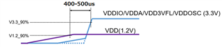
Therefore, customer plans to modify above power sequence as follows. However, customer has some inquiries about this power-up sequence.
- Regarding the improved power-up sequence, VDDIO(3.3V) and VDD(1.2V) is powered up at the same time, but, there is difference in the time to actually power-up(90% voltage). This period is 400-500us. Would you think any issue for this behavior?
- Customer is asking if they need to adjust power-up(90% voltage) time as same time? But, it seems difficult to adjust this timing.
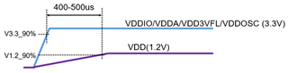
- Regarding above “VDDOSC(3.3V) and VDD(1.2V) must be powered on and off at the same time.”, customer is afraid that it may be spec violation. Would you think any issue for this point?
I tried to summarized their inquiries and attached it(Inquiry about Power up sequence 2023_0427.pdf).
We plans to have face to face meeting tomorrow, so it will be really appreciated if you will share your expert’s advice/comments on them quickly.
Best regards,
Miyazaki
