This thread has been locked.

If you have a related question, please click the "Ask a related question" button in the top right corner. The newly created question will be automatically linked to this question.

TMS320F28335: CPU is not running after power off / on, but it runs after FLASH load

Part Number: TMS320F28335
Other Parts Discussed in Thread: UNIFLASH, C2000WARE

Hello, 

I am following the issue I had on this previous thread https://e2e.ti.com/support/microcontrollers/c2000-microcontrollers-group/c2000/f/c2000-microcontrollers-forum/1225088/tms320f28335-cpu-is-not-running-after-power-off-on-but-it-runs-after-flash-load/4665801, that got closed, but I didn't solve my issue. So complementary issues are here.

Basically, after off / on the power supply of the DSP, the DSP is not running, but it is running after loading the program with Uniflash.

After the last question from , here is what I have found in debug: 

After a CPU reset, my program is waiting here:

and then, after run and halt, it is locked here:

(outside of the program).

I tried to lunch the debug session without performing a reset, and the program is first waiting here:

and then it is working as intended.

Thank you to anyone who can help me,

Have a good day

Best Regars

Matteo

  • Matteo,

    Please give me another day to go back and re-look at everything we did in the last post.  I suspect that the flash entry point is not getting programmed, or we are not jumping to the flash boot entry point as you want.  When we do the flash load, there is a setting in code composer that is taking us straight to main and skipping the BROM, essentially taking care of this for us, so that is why that method works.

    Best,

    Matthew

  • Matteo,

    After you flash the device, can you open a memory browser to 0x33FFF6, can you take a picture of the data at addresses 0x33FFF6 and 0x33FFF7.  This should be the address of your application code(it may not be "main" as there is some pre-main code in the code_start_branch.asm file that happens prior to main).

    The other thing we can try, load and reset(as you did in the first step), but before you run I want to load the boot rom symbols located in C2000Ware here:C:\ti\c2000\C2000Ware_4_03_00_00\libraries\boot_rom\f2833x\v2_0\rom_sources\Debug

    This is under Run->Load, Load symbols.

    We can then single step through the boot rom C code and determine how we are getting in the SB 0, UNC "TRAP" type code.

    Best,

    Matthew

  • Hello Matthey,

    thank you very much for your answers.

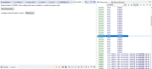
    Here is what I have found with uniflash:

    After flashing the DSP(FFFF in both 0x33FFF6 and 0x33FFF7) :

    In dasassembly in CCS, I have that:

    33fff6: FFFF ITRAP1
    33fff7: FFFF ITRAP1

    I tried to load the boot rom symbols, I didnt see any difference.

    Here is the disassembly recording after reseting the CPU

    Best regards

    Mattéo

  • Mattéo,

    Can you copy your cmd over to this thread(or to make sure it hasn't changed); the fact that this location is all 0xFFFF implies that the linker is not allocating anything to the boot to flash address location; we should see something in the linker that is intentionally assigning these 2 words to a label, usually something like begin, or code_start.

    Best,

    Matthew

  • Hello Matthew, 

    I have noticed this part in my CMD, with begin as you talk about:

    MEMORY
    {
    PAGE 0: /* Program Memory */
    /* Memory (RAM/FLASH/OTP) blocks can be moved to PAGE1 for data allocation */

    ZONE0 : origin = 0x004000, length = 0x001000 /* XINTF zone 0 */
    RAMFUNCS : origin = 0x008000, length = 0x003000 /* on-chip RAM block L0 to L2 */
    ZONE6 : origin = 0x100000, length = 0x100000 /* XINTF zone 6 */
    ZONE7A : origin = 0x200000, length = 0x00FC00 /* XINTF zone 7 - program space */
    BEGIN_FLASH_APPLI : origin = 0x3002FE, length = 0x000002 /* Part of FLASHH. Used for Watt booloader FLASH_APPLIcation entry point. */
    FLASH_APPLI : origin = 0x300300, length = 0x02FD00 /* Part of FLASHH, FLASHG, FLASHF, FLASHE, FLASHD, FLASHC used for application*/
    FLASHA : origin = 0x338000, length = 0x007F80 /* on-chip FLASHA, used for bootloader program */
    CSM_RSVD : origin = 0x33FF80, length = 0x000076 /* Part of FLASHA. Program with all 0x0000 when CSM is in use. */
    BEGIN : origin = 0x33FFF6, length = 0x000002 /* Part of FLASHA. Used for "boot to Flash" bootloader mode. */
    CSM_PWL : origin = 0x33FFF8, length = 0x000008 /* Part of FLASHA. CSM password locations in FLASHA */
    OTP : origi²n = 0x380400, length = 0x000400 /* on-chip OTP */
    ADC_CAL : origin = 0x380080, length = 0x000009 /* ADC_cal function in Reserved memory */

    //IQTABLES : origin = 0x3FE000, length = 0x000b50 /* IQ Math Tables in Boot ROM */
    //IQTABLES2 : origin = 0x3FEB50, length = 0x00008c /* IQ Math Tables in Boot ROM */
    FPUTABLES : origin = 0x3FEBDC, length = 0x0006A0 /* FPU Tables in Boot ROM */
    ROM : origin = 0x3FF27C, length = 0x000D44 /* Boot ROM */
    RESET : origin = 0x3FFFC0, length = 0x000002 /* part of boot ROM */
    VECTORS : origin = 0x3FFFC2, length = 0x00003E /* part of boot ROM */

  • and here a the .cmd files,

    thank you very much 


    /****************************************************************************
    *
    * Copyright (c) 2012 by Watt Consulting
    *
    * This software is copyrighted by and is the sole property of
    * Watt Consulting. All rights, title, ownership, or other interests
    * in the software remain the property of Watt Consulting. This
    * software may only be used in accordance with the corresponding
    * license agreement. Any unauthorized use, duplication, transmission,
    * distribution, or disclosure of this software is expressly forbidden.
    *
    * This Copyright notice may not be removed or modified without prior
    * written consent of Watt Consulting.
    *
    * Watt Consulting reserves the right to modify this software without notice.
    *
    * Watt Consulting
    * 23 rue Alexis de Tocqueville
    * 92160 Antony, FRANCE
    * contact@watt-consulting.com
    ****************************************************************************/

    /****************************************************************************
    *
    * CONFIDENTIAL NOTICE
    *
    * This document contains information confidential and proprietary to
    * Watt Consulting .The information may not be used, disclosed or reproduced
    * without the prior written authorization of Watt Consulting and those so
    * authorized may only use the information for the purpose of evaluation
    * consistent with authorization. Reproduction of any section of this document
    * must include this legend.
    ****************************************************************************/

    //=============================================================================
    ///
    /// @file 28335Application_FLASH.cmd
    ///
    /// @brief Linker command file for flash programming of bootloader
    ///
    /// @author Watt Consulting Team
    //=============================================================================


    MEMORY
    {
    PAGE 0: /* Program Memory */
    /* Memory (RAM/FLASH/OTP) blocks can be moved to PAGE1 for data allocation */

    ZONE0 : origin = 0x004000, length = 0x001000 /* XINTF zone 0 */
    RAMFUNCS : origin = 0x008000, length = 0x003000 /* on-chip RAM block L0 to L2 */
    ZONE6 : origin = 0x100000, length = 0x100000 /* XINTF zone 6 */
    ZONE7A : origin = 0x200000, length = 0x00FC00 /* XINTF zone 7 - program space */
    BEGIN_FLASH_APPLI : origin = 0x3002FE, length = 0x000002 /* Part of FLASHH. Used for Watt booloader FLASH_APPLIcation entry point. */
    FLASH_APPLI : origin = 0x300300, length = 0x02FD00 /* Part of FLASHH, FLASHG, FLASHF, FLASHE, FLASHD, FLASHC used for application*/
    FLASHA : origin = 0x338000, length = 0x007F80 /* on-chip FLASHA, used for bootloader program */
    CSM_RSVD : origin = 0x33FF80, length = 0x000076 /* Part of FLASHA. Program with all 0x0000 when CSM is in use. */
    BEGIN : origin = 0x33FFF6, length = 0x000002 /* Part of FLASHA. Used for "boot to Flash" bootloader mode. */
    CSM_PWL : origin = 0x33FFF8, length = 0x000008 /* Part of FLASHA. CSM password locations in FLASHA */
    OTP : origin = 0x380400, length = 0x000400 /* on-chip OTP */
    ADC_CAL : origin = 0x380080, length = 0x000009 /* ADC_cal function in Reserved memory */

    //IQTABLES : origin = 0x3FE000, length = 0x000b50 /* IQ Math Tables in Boot ROM */
    //IQTABLES2 : origin = 0x3FEB50, length = 0x00008c /* IQ Math Tables in Boot ROM */
    FPUTABLES : origin = 0x3FEBDC, length = 0x0006A0 /* FPU Tables in Boot ROM */
    ROM : origin = 0x3FF27C, length = 0x000D44 /* Boot ROM */
    RESET : origin = 0x3FFFC0, length = 0x000002 /* part of boot ROM */
    VECTORS : origin = 0x3FFFC2, length = 0x00003E /* part of boot ROM */

    PAGE 1 : /* Data Memory */
    /* Memory (RAM/FLASH/OTP) blocks can be moved to PAGE0 for program allocation */
    /* Registers remain on PAGE1 */

    BOOT_RSVD : origin = 0x000000, length = 0x000050 /* Part of M0, BOOT rom will use this for stack */
    RAMM0 : origin = 0x000050, length = 0x0003B0 /* on-chip RAM block M0 */
    RAMM1 : origin = 0x000400, length = 0x000400 /* on-chip RAM block M1 */
    RAMM2 : origin = 0x002000, length = 0x001000 /* on-chip RAM block M2 */
    RAM_GLOBAL_VAR : origin = 0x00B000, length = 0x004B00 /* on-chip RAM block L3 to L6 and part of L7*/
    RAM_ADCRESULT : origin = 0x00FB00, length = 0x000400 /* on-chip RAM block last part of L7*/
    ZONE7B : origin = 0x20FC00, length = 0x000400 /* XINTF zone 7 - data space */
    FLASHB : origin = 0x330000, length = 0x008000 /* on-chip FLASH */
    }

    /* Allocate sections to memory blocks.
    Note:
    codestart user defined section in DSP28_CodeStartBranch.asm used to redirect code
    execution when booting to flash
    ramfuncs user defined section to store functions that will be copied from Flash into RAM
    */

    SECTIONS
    {

    /* Allocate program areas: */
    .cinit : > FLASH_APPLI PAGE = 0
    .pinit : > FLASH_APPLI, PAGE = 0
    .text : > FLASH_APPLI PAGE = 0
    codestart : > BEGIN_FLASH_APPLI PAGE = 0
    ramfuncs : LOAD = FLASH_APPLI,
    RUN = RAMFUNCS,/*RAML0,*/
    LOAD_START(_RamfuncsLoadStart),
    LOAD_END(_RamfuncsLoadEnd),
    RUN_START(_RamfuncsRunStart),
    PAGE = 0


    .FPUtables : LOAD = FLASH_APPLI
    RUN = RAMFUNCS,
    LOAD_START(_FPUtablesLoadStart),
    LOAD_END(_FPUtablesLoadEnd),
    RUN_START(_FPUtablesRunStart),
    PAGE = 0
    {
    -l rts2800_fpu32_fast_supplement.lib
    //-l rts2800_fpu32_fast_supplement_coff.lib
    }

    csmpasswds : > CSM_PWL PAGE = 0
    csm_rsvd : > CSM_RSVD PAGE = 0

    /* Allocate uninitalized data sections: */
    .stack : > RAMM1 PAGE = 1
    .ebss : > RAM_GLOBAL_VAR PAGE = 1
    .esysmem : > RAMM2 PAGE = 1
    .sysmem : > RAM_GLOBAL_VAR PAGE = 1

    /* Initalized sections go in Flash */
    /* For SDFlash to program these, they must be allocated to page 0 */
    .econst : > FLASH_APPLI PAGE = 0
    .switch : > FLASH_APPLI PAGE = 0

    /* Allocate IQ math areas: */
    //IQmath : > FLASH_APPLI PAGE = 0 /* Math Code */
    //IQmathTables : > IQTABLES, PAGE = 0, TYPE = NOLOAD

    /* Uncomment the section below if calling the IQNexp() or IQexp()
    functions from the IQMath.lib library in order to utilize the
    relevant IQ Math table in Boot ROM (This saves space and Boot ROM
    is 1 wait-state). If this section is not uncommented, IQmathTables2
    will be loaded into other memory (SARAM, Flash, etc.) and will take
    up space, but 0 wait-state is possible.
    */
    /*
    IQmathTables2 : > IQTABLES2, PAGE = 0, TYPE = NOLOAD
    {

    IQmath.lib<IQNexpTable.obj> (IQmathTablesRam)

    }
    */

    FPUmathTables : > FPUTABLES, PAGE = 0, TYPE = NOLOAD

    /* Allocate DMA-accessible RAM sections: */
    DMARAML4 : > RAM_ADCRESULT, PAGE = 1
    DMARAML5 : > RAM_ADCRESULT, PAGE = 1
    DMARAML6 : > RAM_ADCRESULT, PAGE = 1
    DMARAML7 : > RAM_ADCRESULT, PAGE = 1

    /* Allocate 0x400 of XINTF Zone 7 to storing data */
    ZONE7DATA : > ZONE7B, PAGE = 1

    /* .reset is a standard section used by the compiler. It contains the */
    /* the address of the start of _c_int00 for C Code. /*
    /* When using the boot ROM this section and the CPU vector */
    /* table is not needed. Thus the default type is set here to */
    /* DSECT */
    .reset : > RESET, PAGE = 0, TYPE = DSECT
    vectors : > VECTORS PAGE = 0, TYPE = DSECT

    /* Allocate ADC_cal function (pre-programmed by factory into TI reserved memory) */
    .adc_cal : load = ADC_CAL, PAGE = 0, TYPE = NOLOAD
    CRC16_TABLE : > RAM_GLOBAL_VAR PAGE = 1
    }
    /*
    //===========================================================================
    // End of file.
    //===========================================================================
    */

    /*
    // TI File $Revision: /main/8 $
    // Checkin $Date: June 2, 2008 11:12:24 $
    //###########################################################################
    //
    // FILE: DSP2833x_Headers_nonBIOS.cmd
    //
    // TITLE: DSP2833x Peripheral registers linker command file
    //
    // DESCRIPTION:
    //
    // This file is for use in Non-BIOS applications.
    //
    // Linker command file to place the peripheral structures
    // used within the DSP2833x headerfiles into the correct memory
    // mapped locations.
    //
    // This version of the file includes the PieVectorTable structure.
    // For BIOS applications, please use the DSP2833x_Headers_BIOS.cmd file
    // which does not include the PieVectorTable structure.
    //
    //###########################################################################
    */

    // Version History:
    //=============================================================================
    // Ver | dd mmm yyyy | Who | Description of changes
    // =====|=============|=======|================================================
    // 1.0 | 02 Jun 2008 | TI | Release Version
    // 2.0 | 06 Sep 2011 | WattC | ePWM mapping changed from 0x68xx to 0x58xx for DMA access
    //=============================================================================

    MEMORY
    {
    PAGE 0: /* Program Memory */

    PAGE 1: /* Data Memory */

    DEV_EMU : origin = 0x000880, length = 0x000180 /* device emulation registers */
    FLASH_REGS : origin = 0x000A80, length = 0x000060 /* FLASH registers */
    CSM : origin = 0x000AE0, length = 0x000010 /* code security module registers */

    ADC_MIRROR : origin = 0x000B00, length = 0x000010 /* ADC Results register mirror */

    XINTF : origin = 0x000B20, length = 0x000020 /* external interface registers */

    CPU_TIMER0 : origin = 0x000C00, length = 0x000008 /* CPU Timer0 registers */
    CPU_TIMER1 : origin = 0x000C08, length = 0x000008 /* CPU Timer0 registers (CPU Timer1 & Timer2 reserved TI use)*/
    CPU_TIMER2 : origin = 0x000C10, length = 0x000008 /* CPU Timer0 registers (CPU Timer1 & Timer2 reserved TI use)*/

    PIE_CTRL : origin = 0x000CE0, length = 0x000020 /* PIE control registers */
    PIE_VECT : origin = 0x000D00, length = 0x000100 /* PIE Vector Table */

    DMA : origin = 0x001000, length = 0x000200 /* DMA registers */

    MCBSPA : origin = 0x005000, length = 0x000040 /* McBSP-A registers */
    MCBSPB : origin = 0x005040, length = 0x000040 /* McBSP-B registers */

    ECANA : origin = 0x006000, length = 0x000040 /* eCAN-A control and status registers */
    ECANA_LAM : origin = 0x006040, length = 0x000040 /* eCAN-A local acceptance masks */
    ECANA_MOTS : origin = 0x006080, length = 0x000040 /* eCAN-A message object time stamps */
    ECANA_MOTO : origin = 0x0060C0, length = 0x000040 /* eCAN-A object time-out registers */
    ECANA_MBOX : origin = 0x006100, length = 0x000100 /* eCAN-A mailboxes */

    ECANB : origin = 0x006200, length = 0x000040 /* eCAN-B control and status registers */
    ECANB_LAM : origin = 0x006240, length = 0x000040 /* eCAN-B local acceptance masks */
    ECANB_MOTS : origin = 0x006280, length = 0x000040 /* eCAN-B message object time stamps */
    ECANB_MOTO : origin = 0x0062C0, length = 0x000040 /* eCAN-B object time-out registers */
    ECANB_MBOX : origin = 0x006300, length = 0x000100 /* eCAN-B mailboxes */

    // EPWM1 : origin = 0x006800, length = 0x000022 /* Enhanced PWM 1 registers */
    // EPWM2 : origin = 0x006840, length = 0x000022 /* Enhanced PWM 2 registers */
    // EPWM3 : origin = 0x006880, length = 0x000022 /* Enhanced PWM 3 registers */
    // EPWM4 : origin = 0x0068C0, length = 0x000022 /* Enhanced PWM 4 registers */
    // EPWM5 : origin = 0x006900, length = 0x000022 /* Enhanced PWM 5 registers */
    // EPWM6 : origin = 0x006940, length = 0x000022 /* Enhanced PWM 6 registers */

    EPWM1 : origin = 0x005800, length = 0x000022 /* Enhanced PWM 1 registers */
    EPWM2 : origin = 0x005840, length = 0x000022 /* Enhanced PWM 2 registers */
    EPWM3 : origin = 0x005880, length = 0x000022 /* Enhanced PWM 3 registers */
    EPWM4 : origin = 0x0058C0, length = 0x000022 /* Enhanced PWM 4 registers */
    EPWM5 : origin = 0x005900, length = 0x000022 /* Enhanced PWM 5 registers */
    EPWM6 : origin = 0x005940, length = 0x000022 /* Enhanced PWM 6 registers */


    ECAP1 : origin = 0x006A00, length = 0x000020 /* Enhanced Capture 1 registers */
    ECAP2 : origin = 0x006A20, length = 0x000020 /* Enhanced Capture 2 registers */
    ECAP3 : origin = 0x006A40, length = 0x000020 /* Enhanced Capture 3 registers */
    ECAP4 : origin = 0x006A60, length = 0x000020 /* Enhanced Capture 4 registers */
    ECAP5 : origin = 0x006A80, length = 0x000020 /* Enhanced Capture 5 registers */
    ECAP6 : origin = 0x006AA0, length = 0x000020 /* Enhanced Capture 6 registers */

    EQEP1 : origin = 0x006B00, length = 0x000040 /* Enhanced QEP 1 registers */
    EQEP2 : origin = 0x006B40, length = 0x000040 /* Enhanced QEP 2 registers */

    GPIOCTRL : origin = 0x006F80, length = 0x000040 /* GPIO control registers */
    GPIODAT : origin = 0x006FC0, length = 0x000020 /* GPIO data registers */
    GPIOINT : origin = 0x006FE0, length = 0x000020 /* GPIO interrupt/LPM registers */

    SYSTEM : origin = 0x007010, length = 0x000020 /* System control registers */
    SPIA : origin = 0x007040, length = 0x000010 /* SPI-A registers */
    SCIA : origin = 0x007050, length = 0x000010 /* SCI-A registers */
    XINTRUPT : origin = 0x007070, length = 0x000010 /* external interrupt registers */

    ADC : origin = 0x007100, length = 0x000020 /* ADC registers */

    SCIB : origin = 0x007750, length = 0x000010 /* SCI-B registers */

    SCIC : origin = 0x007770, length = 0x000010 /* SCI-C registers */

    I2CA : origin = 0x007900, length = 0x000040 /* I2C-A registers */

    CSM_PWL : origin = 0x33FFF8, length = 0x000008 /* Part of FLASHA. CSM password locations. */

    PARTID : origin = 0x380090, length = 0x000001 /* Part ID register location */
    }


    SECTIONS
    {
    PieVectTableFile : > PIE_VECT, PAGE = 1

    /*** Peripheral Frame 0 Register Structures ***/
    DevEmuRegsFile : > DEV_EMU, PAGE = 1
    FlashRegsFile : > FLASH_REGS, PAGE = 1
    CsmRegsFile : > CSM, PAGE = 1
    AdcMirrorFile : > ADC_MIRROR, PAGE = 1
    XintfRegsFile : > XINTF, PAGE = 1
    CpuTimer0RegsFile : > CPU_TIMER0, PAGE = 1
    CpuTimer1RegsFile : > CPU_TIMER1, PAGE = 1
    CpuTimer2RegsFile : > CPU_TIMER2, PAGE = 1
    PieCtrlRegsFile : > PIE_CTRL, PAGE = 1
    DmaRegsFile : > DMA, PAGE = 1

    /*** Peripheral Frame 3 Register Structures ***/
    McbspaRegsFile : > MCBSPA, PAGE = 1
    McbspbRegsFile : > MCBSPB, PAGE = 1

    /*** Peripheral Frame 1 Register Structures ***/
    ECanaRegsFile : > ECANA, PAGE = 1
    ECanaLAMRegsFile : > ECANA_LAM PAGE = 1
    ECanaMboxesFile : > ECANA_MBOX PAGE = 1
    ECanaMOTSRegsFile : > ECANA_MOTS PAGE = 1
    ECanaMOTORegsFile : > ECANA_MOTO PAGE = 1

    ECanbRegsFile : > ECANB, PAGE = 1
    ECanbLAMRegsFile : > ECANB_LAM PAGE = 1
    ECanbMboxesFile : > ECANB_MBOX PAGE = 1
    ECanbMOTSRegsFile : > ECANB_MOTS PAGE = 1
    ECanbMOTORegsFile : > ECANB_MOTO PAGE = 1

    EPwm1RegsFile : > EPWM1 PAGE = 1
    EPwm2RegsFile : > EPWM2 PAGE = 1
    EPwm3RegsFile : > EPWM3 PAGE = 1
    EPwm4RegsFile : > EPWM4 PAGE = 1
    EPwm5RegsFile : > EPWM5 PAGE = 1
    EPwm6RegsFile : > EPWM6 PAGE = 1

    ECap1RegsFile : > ECAP1 PAGE = 1
    ECap2RegsFile : > ECAP2 PAGE = 1
    ECap3RegsFile : > ECAP3 PAGE = 1
    ECap4RegsFile : > ECAP4 PAGE = 1
    ECap5RegsFile : > ECAP5 PAGE = 1
    ECap6RegsFile : > ECAP6 PAGE = 1

    EQep1RegsFile : > EQEP1 PAGE = 1
    EQep2RegsFile : > EQEP2 PAGE = 1

    GpioCtrlRegsFile : > GPIOCTRL PAGE = 1
    GpioDataRegsFile : > GPIODAT PAGE = 1
    GpioIntRegsFile : > GPIOINT PAGE = 1

    /*** Peripheral Frame 2 Register Structures ***/
    SysCtrlRegsFile : > SYSTEM, PAGE = 1
    SpiaRegsFile : > SPIA, PAGE = 1
    SciaRegsFile : > SCIA, PAGE = 1
    XIntruptRegsFile : > XINTRUPT, PAGE = 1
    AdcRegsFile : > ADC, PAGE = 1
    ScibRegsFile : > SCIB, PAGE = 1
    ScicRegsFile : > SCIC, PAGE = 1
    I2caRegsFile : > I2CA, PAGE = 1

    /*** Code Security Module Register Structures ***/
    CsmPwlFile : > CSM_PWL, PAGE = 1

    /*** Device Part ID Register Structures ***/
    PartIdRegsFile : > PARTID, PAGE = 1

    }


    /*
    //===========================================================================
    // End of file.
    //===========================================================================
    */


    /****************************************************************************
    *
    * Copyright (c) 2012 by Watt Consulting
    *
    * This software is copyrighted by and is the sole property of
    * Watt Consulting. All rights, title, ownership, or other interests
    * in the software remain the property of Watt Consulting. This
    * software may only be used in accordance with the corresponding
    * license agreement. Any unauthorized use, duplication, transmission,
    * distribution, or disclosure of this software is expressly forbidden.
    *
    * This Copyright notice may not be removed or modified without prior
    * written consent of Watt Consulting.
    *
    * Watt Consulting reserves the right to modify this software without notice.
    *
    * Watt Consulting
    * 23 rue Alexis de Tocqueville
    * 92160 Antony, FRANCE
    * contact@watt-consulting.com
    ****************************************************************************/

    /****************************************************************************
    *
    * CONFIDENTIAL NOTICE
    *
    * This document contains information confidential and proprietary to
    * Watt Consulting .The information may not be used, disclosed or reproduced
    * without the prior written authorization of Watt Consulting and those so
    * authorized may only use the information for the purpose of evaluation
    * consistent with authorization. Reproduction of any section of this document
    * must include this legend.
    ****************************************************************************/

    //=============================================================================
    ///
    /// @file MetadataHeader.cmd
    ///
    /// @brief Linker command file for metadata shared between Bootloader and Application
    ///
    /// @author Watt Consulting Team
    //=============================================================================

    MEMORY
    {
    PAGE 0: /* Program Memory */

    UPGRADE_METADATA : origin = 0x300000, length = 0x000004 /* upgrade metadata registers */
    APPLICATION_METADATA : origin = 0x300004, length = 0x0002FA /* upgrade metadata registers */

    PAGE 1: /* Data Memory */


    }


    SECTIONS
    {
    UpgradeMetadataFile : > UPGRADE_METADATA , PAGE = 0
    ApplicationMetadataFile : > APPLICATION_METADATA, PAGE = 0

    SharedDataFile : > RAMM0 , PAGE = 1
    }


    /*
    //===========================================================================
    // End of file.
    //===========================================================================
    */

  • Matteo,

    in the sections of the 1st .cmd file code start needs to be assigned to “begin” as that is the address that the boot rom will use to branch into your code.  The code_start.asm will then branch to main.

    best,

    matt

  • Hello Matthew, 

    I tried to put 0x303348 adress in begin, because it should be my entry point according to this picture:

    But I've got this error:

    BEGIN memory range overlaps existing memory range FLASH_APPLI

    Giving you my cmd file again:

    ZONE0 : origin = 0x004000, length = 0x001000 /* XINTF zone 0 */
    RAMFUNCS : origin = 0x008000, length = 0x003000 /* on-chip RAM block L0 to L2 */
    ZONE6 : origin = 0x100000, length = 0x100000 /* XINTF zone 6 */
    ZONE7A : origin = 0x200000, length = 0x00FC00 /* XINTF zone 7 - program space */
    BEGIN_FLASH_APPLI : origin = 0x3002FE, length = 0x000002 /* Part of FLASHH. Used for Watt booloader FLASH_APPLIcation entry point. */
    FLASH_APPLI : origin = 0x300300, length = 0x02FD00 /* Part of FLASHH, FLASHG, FLASHF, FLASHE, FLASHD, FLASHC used for application*/
    FLASHA : origin = 0x338000, length = 0x007F80 /* on-chip FLASHA, used for bootloader program */
    CSM_RSVD : origin = 0x33FF80, length = 0x000076 /* Part of FLASHA. Program with all 0x0000 when CSM is in use. */
    BEGIN : origin = 0x303348, length = 0x000002 /* Part of FLASHA. Used for "boot to Flash" bootloader mode. */
    CSM_PWL : origin = 0x33FFF8, length = 0x000008 /* Part of FLASHA. CSM password locations in FLASHA */
    OTP : origin = 0x380400, length = 0x000400 /* on-chip OTP */
    ADC_CAL : origin = 0x380080, length = 0x000009 /* ADC_cal function in Reserved memory */

    What should I put in FLASH APPLI ?

    Best regards

    Mattéo

  • Matteo,

    You can remove the BEGIN_FLASH_APPLI section from the top portion of the linker; and just assign FLASH_APPLI to .text as you have it.

    New section of the linker would look like this:

    /* Allocate program areas: */
    .cinit : > FLASH_APPLI PAGE = 0
    .pinit : > FLASH_APPLI, PAGE = 0
    .text : > FLASH_APPLI PAGE = 0
    codestart : > BEGIN PAGE = 0

    I want to call attention to the next few lines:

    ramfuncs : LOAD = FLASH_APPLI,
    RUN = RAMFUNCS,/*RAML0,*/

    We cannot assign the entire FLASH_APPLI to be a load/run.  This is because we need some portion of the "main" to execute the code copy from flash to RAM before running from RAM.

    If we go back you could keep the BEGIN_FLASH_APPLI section for this, and make sure to include the copy from flash to RAM, before the FLASH_APPLI section occurs in the code; likely this would mean you need one more function inside main that contains the bulk of your code functions so that it can be placed/copied accordingly.

    So, the code_start.asm function will be placed at the initial boot from flash address vector.  When that function completes it will automatically call the c_int(which is assigned to main()).  At this point you can do whatever setup of the C28x you want (set up the clocks, ISRs, etc); then call the copy code function to put your time critical code into RAM, then call that function which will then jump to that function in RAM.

    Best,

    Matthew

  • Matthew,

    Before going in the second part of your message, the first part didn't solve my issue.

    The overlap I have, when putting main's adress in BEGIN is with FLASH APPLI, so removing BEGIN_FLASH_APPLi didn't solve my issue.

    Sorry for all my questions, it is my first time dealing with linker files.

    Thank you

    Mattéo 

  • Hello Matthew,

    I am coming back to you, since I am still locked because of my previous answer. Do you have any idea ?

    Thank you

    Mattéo

  • Hi Matteo,

    The expert is out of office today, please expect a response back by tomorrow.

    Thank you,

    Luke

  • Hello Luke,

    Thank you for the information

  • Matteo,

    Would it be possible to remove the load to flash and run from RAM and just place in flash?  I realized that the code execution will be slower, but I want to get to a state that we can flash the code, and boot up successfully.

    In this case you would remove the BEGIN_FLASH_APPL section from the  linker command file, and just place the FLASH APPLI(or really there is no label needed here, since this is code)/.text into flash.

    We need to keep the codestart : > BEGIN PAGE = 0; as this is coming from the code_start_branch.asm and need to be placed at the reset vector location to run first at boot.

    Best,

    Matthew

  • Hello Matthew, 

    just place the FLASH APPLI(or really there is no label needed here, since this is code)/.text into flash.

    What do you mean here ? I indeed removed BEGIN_FLASH_APPLI, and put codestart : > BEGIN, but I still can't change BEGIN origin because of the overlap with FLASH APPLI, so I don't understand where I should place FLASH APPLI. I can't either remove FLASH APPLI, because of theses errors...

    "../cmd/28335Application_FLASH.cmd", line 131: error #10265: no valid memory range available for placement of ".switch"
    "../cmd/28335Application_FLASH.cmd", line 131: error #10099-D: program will not fit into available memory, or the section contains a call site that requires a trampoline that can't be generated for this section. placement with alignment/blocking fails for section ".switch" size 0x4a page 0

    Thank you,

    Mattéo

  • If we add back in the 2 words that were in the BEGIN_FLASH_APPLI, that should give us equivalent room

    BEGIN_FLASH_APPLI : origin = 0x3002FE, length = 0x000002 /* Part of FLASHH. Used for Watt booloader FLASH_APPLIcation entry point. */
    FLASH_APPLI : origin = 0x300300, length = 0x02FD00 /* Part of FLASHH, FLASHG, FLASHF, FLASHE, FLASHD, FLASHC used for application*/

    change to

    FLASH_APPLI: origin = 0x3002FE, length = 0x02FD02

    I hadn't considered that FLASH_APPLI would be at 100% utilization.

    Can you show me what code was in BEGIN_FLASH_APPLI, originally?  I'm assuming this was just a branch/call?  If so, that won't be needed since FLASH_APPLI will get a branch from code_start_branch.asm.

    Best,
    Matt

  • Ok, I tried this change, with codestart :> begin

    BEGIN_FLASH_APPLI : origin = 0x3002FE, length = 0x000002 /* Part of FLASHH. Used for Watt booloader FLASH_APPLIcation entry point. */
    FLASH_APPLI : origin = 0x300300, length = 0x02FD00 /* Part of FLASHH, FLASHG, FLASHF, FLASHE, FLASHD, FLASHC used for application*/

    change to

    FLASH_APPLI: origin = 0x3002FE, length = 0x02FD02

    and I still have the issue after an off / on with the power supply. I'm assuming that this is because I don't have the good adress in begin (main() adress is 303348, and in begin I have 0x33FFF6 adress).

    Can you show me what code was in BEGIN_FLASH_APPLI, originally?

    And I wen't to begin FLASH APPLI adress, and here is what I have:

    Mattéo

  • Matteo,

    If you reset the device, and then put a break point at address 0x33FFF6 and run, you should be halted in the code_start_branch.asm(verify this first).

    The last instruction of the code_start_branch should be to do a function call to your main 0x3002FE.

    Let's see what is different when your code executes.

    Best,
    Matthew

  • Matthew,

    Here is what I have at 0x33FFF6, not looking code_start_branch.asm.. (ITRAP1 in dasassembly / "Break at address "0x33fff6" with no debug information available, or outside of program code.")

    Thank you

    Mattéo

  • Mattéo,

    This should not be possible given the .cmd we are working with.  Basically nothing is getting loaded here, and this will cause the BROM to fetch an illegal instruction.

    Can you build and load the example in C2000Ware here: C:\ti\c2000\C2000Ware_5_00_00_00\device_support\f2833x\examples\flash_f28335

    and then look at the same 0x33FFF6 address and verify that we see code_start_branch loaded there?

    Best,

    Matthew

  • Hello Matthew,

    Just for you information, I will be out of the office for more than 3 weeks, so I won't be able to continue working on that.

    But please, keep the thread opened, I will update the thread as soon as I come back.

    Thank you,

    Mattéo

  • Hello Matthew,

    Sory for the delay, I am back.

    With the flash_f28335 software, here is what I have in 33FFF6 after a reset:

    and then, after running the program, everything is still fine....

    So the issue is only with my own program.

    Mattéo

  • Mattéo,

    Thanks for the update; can you compare the .cmd files from this example and your project and see if there are changes we can make to align with the example?

    Best,

    Matthew

  • Hello, 

    There is this difference:

    In the example:

    SECTIONS
    {

    /* Allocate program areas: */
    .cinit : > FLASHA PAGE = 0
    .pinit : > FLASHA, PAGE = 0
    .text : > FLASHA PAGE = 0
    codestart : > BEGIN PAGE = 0

    In my file ;

    SECTIONS
    {

    /* Allocate program areas: */
    .cinit : > FLASH_APPLI PAGE = 0
    .pinit : > FLASH_APPLI, PAGE = 0
    .text : > FLASH_APPLI PAGE = 0
    codestart : > BEGIN_FLASH_APPLI PAGE = 0

    I changed it in my file to match the example, it didn't work.

    I also chat GPT'ed all the files, are is his answer : 

    1. Memory Definitions:

      • The memory layout has been significantly modified. Addresses and lengths of various memory sections have been changed or rearranged.
      • New memory sections like RAMFUNCS, RAM_GLOBAL_VAR, RAM_ADCRESULT, RAMM2, FLASH_APPLI, RAMM2, FLASH_APPLI, and more have been introduced.
      • Memory addresses of several existing sections like ZONE0, ZONE6, ZONE7A, FLASHA, BEGIN, CSM_PWL, OTP, IQTABLES, IQTABLES2, FPUTABLES, ROM, RESET, VECTORS, BOOT_RSVD, RAMM0, RAMM1, ZONE7B, FLASHB, FLASH_REGS, CSM, ADC_MIRROR, XINTF, CPU_TIMER0, CPU_TIMER1, CPU_TIMER2, PIE_CTRL, DMA, and more have been changed.
      • Certain sections like IQTABLES and IQTABLES2 have been commented out in the second file.
    2. Section Allocation:

      • The section allocation for several areas has been changed. Sections like .cinit, .pinit, .text, codestart, ramfuncs, FPUtables, csmpasswds, .stack, .ebss, .esysmem, .sysmem, .econst, .switch, IQmath, IQmathTables, FPUmathTables, DMARAML4, DMARAML5, DMARAML6, DMARAML7, ZONE7DATA, .reset, vectors, and .adc_cal have been updated with new memory locations.
    3. Peripheral Register Definitions:

      • The registers for various peripherals such as DevEmuRegsFile, FlashRegsFile, CsmRegsFile, AdcMirrorFile, XintfRegsFile, CpuTimer0RegsFile, CpuTimer1RegsFile, CpuTimer2RegsFile, PieCtrlRegsFile, DmaRegsFile, McbspaRegsFile, McbspbRegsFile, ECanaRegsFile, ECanaLAMRegsFile, ECanaMboxesFile, ECanaMOTSRegsFile, ECanaMOTORegsFile, ECanbRegsFile, ECanbLAMRegsFile, ECanbMboxesFile, ECanbMOTSRegsFile, ECanbMOTORegsFile, EPwm1RegsFile, EPwm2RegsFile, EPwm3RegsFile, EPwm4RegsFile, EPwm5RegsFile, EPwm6RegsFile, ECap1RegsFile, ECap2RegsFile, ECap3RegsFile, ECap4RegsFile, ECap5RegsFile, ECap6RegsFile, EQep1RegsFile, EQep2RegsFile, GpioCtrlRegsFile, GpioDataRegsFile, GpioIntRegsFile, SysCtrlRegsFile, SpiaRegsFile, SciaRegsFile, XIntruptRegsFile, AdcRegsFile, ScibRegsFile, ScicRegsFile, and I2caRegsFile have been assigned to specific memory sections.
    4. PartID Definition:

      • The definition for the PartID register location has been modified

    I am giving you again my linker files

    /****************************************************************************
     *
     *            Copyright (c) 2012 by Watt Consulting
     *
     * This software is copyrighted by and is the sole property of
     * Watt Consulting.  All rights, title, ownership, or other interests
     * in the software remain the property of Watt Consulting.  This
     * software may only be used in accordance with the corresponding
     * license agreement.  Any unauthorized use, duplication, transmission, 
     * distribution, or disclosure of this software is expressly forbidden.
     *
     * This Copyright notice may not be removed or modified without prior
     * written consent of Watt Consulting.
     *
     * Watt Consulting reserves the right to modify this software without notice.
     *
     * Watt Consulting
     * 23 rue  Alexis de Tocqueville
     * 92160 Antony, FRANCE
     * contact@watt-consulting.com
     ****************************************************************************/
     
    /****************************************************************************
     *
     *						CONFIDENTIAL NOTICE
     *
     * This document contains information confidential and proprietary to 
     * Watt Consulting .The information may not be used, disclosed or reproduced 
     * without the prior written authorization of Watt Consulting and those so 
     * authorized may only use the information for the purpose of evaluation 
     * consistent with authorization. Reproduction of any section of this document
     *  must include this legend.
     ****************************************************************************/
    
    //=============================================================================
    ///
    /// @file	28335Application_FLASH.cmd
    ///
    /// @brief	Linker command file for flash programming of bootloader
    ///
    /// @author	Watt Consulting Team
    //=============================================================================
    
    
    MEMORY
    {
    PAGE 0:    /* Program Memory */
               /* Memory (RAM/FLASH/OTP) blocks can be moved to PAGE1 for data allocation */
    
       ZONE0      		 	: origin = 0x004000, length = 0x001000     /* XINTF zone 0 */
       RAMFUNCS   			: origin = 0x008000, length = 0x003000     /* on-chip RAM block L0 to L2 */
       ZONE6       			: origin = 0x100000, length = 0x100000     /* XINTF zone 6 */
       ZONE7A      			: origin = 0x200000, length = 0x00FC00     /* XINTF zone 7 - program space */
       BEGIN_FLASH_APPLI 	: origin = 0x3002FE, length = 0x000002     /* Part of FLASHH.  Used for Watt booloader FLASH_APPLIcation entry point. */
       FLASH_APPLI 			: origin = 0x300300, length = 0x02FD00     /* Part of FLASHH, FLASHG, FLASHF, FLASHE, FLASHD, FLASHC  used for application*/
       FLASHA      			: origin = 0x338000, length = 0x007F80     /* on-chip FLASHA, used for bootloader program */
       CSM_RSVD    			: origin = 0x33FF80, length = 0x000076     /* Part of FLASHA.  Program with all 0x0000 when CSM is in use. */
       BEGIN       			: origin = 0x33FFF6, length = 0x000002     /* Part of FLASHA.  Used for "boot to Flash" bootloader mode. */
       CSM_PWL    			: origin = 0x33FFF8, length = 0x000008     /* Part of FLASHA.  CSM password locations in FLASHA */
       OTP         			: origin = 0x380400, length = 0x000400     /* on-chip OTP */
       ADC_CAL     			: origin = 0x380080, length = 0x000009     /* ADC_cal function in Reserved memory */
       
       //IQTABLES    			: origin = 0x3FE000, length = 0x000b50     /* IQ Math Tables in Boot ROM */
       //IQTABLES2   			: origin = 0x3FEB50, length = 0x00008c     /* IQ Math Tables in Boot ROM */
       FPUTABLES   			: origin = 0x3FEBDC, length = 0x0006A0     /* FPU Tables in Boot ROM */
       ROM         			: origin = 0x3FF27C, length = 0x000D44     /* Boot ROM */        
       RESET       			: origin = 0x3FFFC0, length = 0x000002     /* part of boot ROM  */
       VECTORS     			: origin = 0x3FFFC2, length = 0x00003E     /* part of boot ROM  */
    
    PAGE 1 :   /* Data Memory */
               /* Memory (RAM/FLASH/OTP) blocks can be moved to PAGE0 for program allocation */
               /* Registers remain on PAGE1                                                  */
       
       BOOT_RSVD   			: origin = 0x000000, length = 0x000050     /* Part of M0, BOOT rom will use this for stack */
       RAMM0       			: origin = 0x000050, length = 0x0003B0     /* on-chip RAM block M0 */
       RAMM1       			: origin = 0x000400, length = 0x000400     /* on-chip RAM block M1 */
       RAMM2       			: origin = 0x002000, length = 0x001000     /* on-chip RAM block M2 */
       RAM_GLOBAL_VAR       : origin = 0x00B000, length = 0x004B00     /* on-chip RAM block L3 to L6 and part of L7*/
       RAM_ADCRESULT   		: origin = 0x00FB00, length = 0x000400     /* on-chip RAM block last part of L7*/
       ZONE7B      			: origin = 0x20FC00, length = 0x000400     /* XINTF zone 7 - data space */
       FLASHB      			: origin = 0x330000, length = 0x008000     /* on-chip FLASH */
    }
    
    /* Allocate sections to memory blocks.
       Note:
             codestart user defined section in DSP28_CodeStartBranch.asm used to redirect code 
                       execution when booting to flash
             ramfuncs  user defined section to store functions that will be copied from Flash into RAM
    */ 
     
    SECTIONS
    {
     
       /* Allocate program areas: */
       .cinit              : > FLASH_APPLI      PAGE = 0
       .pinit              : > FLASH_APPLI,     PAGE = 0
       .text               : > FLASH_APPLI      PAGE = 0
       codestart           : > BEGIN_FLASH_APPLI       PAGE = 0
       ramfuncs            : LOAD = FLASH_APPLI,
                             RUN = RAMFUNCS,/*RAML0,*/
                             LOAD_START(_RamfuncsLoadStart),
                             LOAD_END(_RamfuncsLoadEnd),
                             RUN_START(_RamfuncsRunStart),
                             PAGE = 0
    
    
    	.FPUtables : LOAD = FLASH_APPLI
    		RUN = RAMFUNCS,
    		LOAD_START(_FPUtablesLoadStart),
    		LOAD_END(_FPUtablesLoadEnd),
    		RUN_START(_FPUtablesRunStart),
    		PAGE = 0
    		{
    		 -l rts2800_fpu32_fast_supplement.lib
    		 //-l rts2800_fpu32_fast_supplement_coff.lib
    		}
    
       csmpasswds          : > CSM_PWL     PAGE = 0
       csm_rsvd            : > CSM_RSVD    PAGE = 0
       
       /* Allocate uninitalized data sections: */
       .stack              : > RAMM1       PAGE = 1
       .ebss               : > RAM_GLOBAL_VAR    PAGE = 1
       .esysmem            : > RAMM2       PAGE = 1
       .sysmem             : > RAM_GLOBAL_VAR   PAGE = 1
    
       /* Initalized sections go in Flash */
       /* For SDFlash to program these, they must be allocated to page 0 */
       .econst             : > FLASH_APPLI      PAGE = 0
       .switch             : > FLASH_APPLI      PAGE = 0
    
       /* Allocate IQ math areas: */
       //IQmath              : > FLASH_APPLI      PAGE = 0                  /* Math Code */
       //IQmathTables     : > IQTABLES,  PAGE = 0, TYPE = NOLOAD
    
       /* Uncomment the section below if calling the IQNexp() or IQexp()
          functions from the IQMath.lib library in order to utilize the
          relevant IQ Math table in Boot ROM (This saves space and Boot ROM
          is 1 wait-state). If this section is not uncommented, IQmathTables2
          will be loaded into other memory (SARAM, Flash, etc.) and will take
          up space, but 0 wait-state is possible.
       */
       /*
       IQmathTables2    : > IQTABLES2, PAGE = 0, TYPE = NOLOAD
       {
    
                  IQmath.lib<IQNexpTable.obj> (IQmathTablesRam)
    
       }
       */
    
       FPUmathTables    : > FPUTABLES, PAGE = 0, TYPE = NOLOAD
             
       /* Allocate DMA-accessible RAM sections: */
       DMARAML4         : > RAM_ADCRESULT,     PAGE = 1
       DMARAML5         : > RAM_ADCRESULT,     PAGE = 1
       DMARAML6         : > RAM_ADCRESULT,     PAGE = 1
       DMARAML7         : > RAM_ADCRESULT,     PAGE = 1
       
       /* Allocate 0x400 of XINTF Zone 7 to storing data */
       ZONE7DATA        : > ZONE7B,    PAGE = 1
    
       /* .reset is a standard section used by the compiler.  It contains the */ 
       /* the address of the start of _c_int00 for C Code.   /*
       /* When using the boot ROM this section and the CPU vector */
       /* table is not needed.  Thus the default type is set here to  */
       /* DSECT  */ 
       .reset              : > RESET,      PAGE = 0, TYPE = DSECT
       vectors             : > VECTORS     PAGE = 0, TYPE = DSECT
       
       /* Allocate ADC_cal function (pre-programmed by factory into TI reserved memory) */
       .adc_cal     : load = ADC_CAL,   PAGE = 0, TYPE = NOLOAD
    	CRC16_TABLE			: > RAM_GLOBAL_VAR				PAGE = 1
    }
    /*
    //===========================================================================
    // End of file.
    //===========================================================================
    */


    /*
    // TI File $Revision: /main/8 $
    // Checkin $Date: June 2, 2008   11:12:24 $
    //###########################################################################
    //
    // FILE:    DSP2833x_Headers_nonBIOS.cmd
    //
    // TITLE:   DSP2833x Peripheral registers linker command file 
    //
    // DESCRIPTION: 
    // 
    //          This file is for use in Non-BIOS applications.
    //
    //          Linker command file to place the peripheral structures 
    //          used within the DSP2833x headerfiles into the correct memory
    //          mapped locations.
    //
    //          This version of the file includes the PieVectorTable structure.
    //          For BIOS applications, please use the DSP2833x_Headers_BIOS.cmd file
    //          which does not include the PieVectorTable structure.
    //
    //###########################################################################
    */
    
    // Version History:
    //=============================================================================
    //  Ver | dd mmm yyyy | Who   | Description of changes
    // =====|=============|=======|================================================
    //  1.0 | 02 Jun 2008 | TI    | Release Version
    //	2.0	| 06 Sep 2011 | WattC | ePWM mapping changed from 0x68xx to 0x58xx for DMA access
    //=============================================================================


    MEMORY
    {
     PAGE 0:    /* Program Memory */
    
     PAGE 1:    /* Data Memory */
     
       DEV_EMU     : origin = 0x000880, length = 0x000180     /* device emulation registers */
       FLASH_REGS  : origin = 0x000A80, length = 0x000060     /* FLASH registers */
       CSM         : origin = 0x000AE0, length = 0x000010     /* code security module registers */
      
       ADC_MIRROR  : origin = 0x000B00, length = 0x000010     /* ADC Results register mirror */
    
       XINTF       : origin = 0x000B20, length = 0x000020     /* external interface registers */
       
       CPU_TIMER0  : origin = 0x000C00, length = 0x000008     /* CPU Timer0 registers */
       CPU_TIMER1  : origin = 0x000C08, length = 0x000008     /* CPU Timer0 registers (CPU Timer1 & Timer2 reserved TI use)*/
       CPU_TIMER2  : origin = 0x000C10, length = 0x000008     /* CPU Timer0 registers (CPU Timer1 & Timer2 reserved TI use)*/
    
       PIE_CTRL    : origin = 0x000CE0, length = 0x000020     /* PIE control registers */
       PIE_VECT    : origin = 0x000D00, length = 0x000100     /* PIE Vector Table */
    
       DMA         : origin = 0x001000, length = 0x000200     /* DMA registers */
    
       MCBSPA      : origin = 0x005000, length = 0x000040     /* McBSP-A registers */
       MCBSPB      : origin = 0x005040, length = 0x000040     /* McBSP-B registers */
    
       ECANA       : origin = 0x006000, length = 0x000040     /* eCAN-A control and status registers */ 
       ECANA_LAM   : origin = 0x006040, length = 0x000040     /* eCAN-A local acceptance masks */
       ECANA_MOTS  : origin = 0x006080, length = 0x000040     /* eCAN-A message object time stamps */
       ECANA_MOTO  : origin = 0x0060C0, length = 0x000040     /* eCAN-A object time-out registers */
       ECANA_MBOX  : origin = 0x006100, length = 0x000100     /* eCAN-A mailboxes */
    
       ECANB       : origin = 0x006200, length = 0x000040     /* eCAN-B control and status registers */ 
       ECANB_LAM   : origin = 0x006240, length = 0x000040     /* eCAN-B local acceptance masks */
       ECANB_MOTS  : origin = 0x006280, length = 0x000040     /* eCAN-B message object time stamps */
       ECANB_MOTO  : origin = 0x0062C0, length = 0x000040     /* eCAN-B object time-out registers */
       ECANB_MBOX  : origin = 0x006300, length = 0x000100     /* eCAN-B mailboxes */
    
    //   EPWM1       : origin = 0x006800, length = 0x000022     /* Enhanced PWM 1 registers */
    //   EPWM2       : origin = 0x006840, length = 0x000022     /* Enhanced PWM 2 registers */
    //   EPWM3       : origin = 0x006880, length = 0x000022     /* Enhanced PWM 3 registers */
    //   EPWM4       : origin = 0x0068C0, length = 0x000022     /* Enhanced PWM 4 registers */
    //   EPWM5       : origin = 0x006900, length = 0x000022     /* Enhanced PWM 5 registers */
    //   EPWM6       : origin = 0x006940, length = 0x000022     /* Enhanced PWM 6 registers */
    
       EPWM1       : origin = 0x005800, length = 0x000022     /* Enhanced PWM 1 registers */
       EPWM2       : origin = 0x005840, length = 0x000022     /* Enhanced PWM 2 registers */
       EPWM3       : origin = 0x005880, length = 0x000022     /* Enhanced PWM 3 registers */
       EPWM4       : origin = 0x0058C0, length = 0x000022     /* Enhanced PWM 4 registers */
       EPWM5       : origin = 0x005900, length = 0x000022     /* Enhanced PWM 5 registers */
       EPWM6       : origin = 0x005940, length = 0x000022     /* Enhanced PWM 6 registers */
    
    
       ECAP1       : origin = 0x006A00, length = 0x000020     /* Enhanced Capture 1 registers */
       ECAP2       : origin = 0x006A20, length = 0x000020     /* Enhanced Capture 2 registers */
       ECAP3       : origin = 0x006A40, length = 0x000020     /* Enhanced Capture 3 registers */
       ECAP4       : origin = 0x006A60, length = 0x000020     /* Enhanced Capture 4 registers */         
       ECAP5       : origin = 0x006A80, length = 0x000020     /* Enhanced Capture 5 registers */         
       ECAP6       : origin = 0x006AA0, length = 0x000020     /* Enhanced Capture 6 registers */         
     
       EQEP1       : origin = 0x006B00, length = 0x000040     /* Enhanced QEP 1 registers */
       EQEP2       : origin = 0x006B40, length = 0x000040     /* Enhanced QEP 2 registers */   
    
       GPIOCTRL    : origin = 0x006F80, length = 0x000040     /* GPIO control registers */
       GPIODAT     : origin = 0x006FC0, length = 0x000020     /* GPIO data registers */
       GPIOINT     : origin = 0x006FE0, length = 0x000020     /* GPIO interrupt/LPM registers */
                     
       SYSTEM      : origin = 0x007010, length = 0x000020     /* System control registers */
       SPIA        : origin = 0x007040, length = 0x000010     /* SPI-A registers */
       SCIA        : origin = 0x007050, length = 0x000010     /* SCI-A registers */
       XINTRUPT    : origin = 0x007070, length = 0x000010     /* external interrupt registers */
    
       ADC         : origin = 0x007100, length = 0x000020     /* ADC registers */
    
       SCIB        : origin = 0x007750, length = 0x000010     /* SCI-B registers */
    
       SCIC        : origin = 0x007770, length = 0x000010     /* SCI-C registers */
       
       I2CA        : origin = 0x007900, length = 0x000040     /* I2C-A registers */
       
       CSM_PWL     : origin = 0x33FFF8, length = 0x000008     /* Part of FLASHA.  CSM password locations. */
    
       PARTID      : origin = 0x380090, length = 0x000001     /* Part ID register location */
    }
    
     
    SECTIONS
    {
       PieVectTableFile : > PIE_VECT,   PAGE = 1
    
    /*** Peripheral Frame 0 Register Structures ***/
       DevEmuRegsFile    : > DEV_EMU,     PAGE = 1
       FlashRegsFile     : > FLASH_REGS,  PAGE = 1
       CsmRegsFile       : > CSM,         PAGE = 1
       AdcMirrorFile     : > ADC_MIRROR,  PAGE = 1 
       XintfRegsFile     : > XINTF,       PAGE = 1
       CpuTimer0RegsFile : > CPU_TIMER0,  PAGE = 1
       CpuTimer1RegsFile : > CPU_TIMER1,  PAGE = 1
       CpuTimer2RegsFile : > CPU_TIMER2,  PAGE = 1  
       PieCtrlRegsFile   : > PIE_CTRL,    PAGE = 1     
       DmaRegsFile       : > DMA,         PAGE = 1 
    
    /*** Peripheral Frame 3 Register Structures ***/
       McbspaRegsFile    : > MCBSPA,      PAGE = 1
       McbspbRegsFile    : > MCBSPB,      PAGE = 1
    
    /*** Peripheral Frame 1 Register Structures ***/
       ECanaRegsFile     : > ECANA,       PAGE = 1
       ECanaLAMRegsFile  : > ECANA_LAM    PAGE = 1   
       ECanaMboxesFile   : > ECANA_MBOX   PAGE = 1
       ECanaMOTSRegsFile : > ECANA_MOTS   PAGE = 1
       ECanaMOTORegsFile : > ECANA_MOTO   PAGE = 1
       
       ECanbRegsFile     : > ECANB,       PAGE = 1
       ECanbLAMRegsFile  : > ECANB_LAM    PAGE = 1   
       ECanbMboxesFile   : > ECANB_MBOX   PAGE = 1
       ECanbMOTSRegsFile : > ECANB_MOTS   PAGE = 1
       ECanbMOTORegsFile : > ECANB_MOTO   PAGE = 1
       
       EPwm1RegsFile     : > EPWM1        PAGE = 1   
       EPwm2RegsFile     : > EPWM2        PAGE = 1   
       EPwm3RegsFile     : > EPWM3        PAGE = 1   
       EPwm4RegsFile     : > EPWM4        PAGE = 1   
       EPwm5RegsFile     : > EPWM5        PAGE = 1   
       EPwm6RegsFile     : > EPWM6        PAGE = 1
       
       ECap1RegsFile     : > ECAP1        PAGE = 1   
       ECap2RegsFile     : > ECAP2        PAGE = 1   
       ECap3RegsFile     : > ECAP3        PAGE = 1   
       ECap4RegsFile     : > ECAP4        PAGE = 1
       ECap5RegsFile     : > ECAP5        PAGE = 1   
       ECap6RegsFile     : > ECAP6        PAGE = 1
    
       EQep1RegsFile     : > EQEP1        PAGE = 1   
       EQep2RegsFile     : > EQEP2        PAGE = 1               
    
       GpioCtrlRegsFile  : > GPIOCTRL     PAGE = 1
       GpioDataRegsFile  : > GPIODAT      PAGE = 1
       GpioIntRegsFile   : > GPIOINT      PAGE = 1
       
    /*** Peripheral Frame 2 Register Structures ***/
       SysCtrlRegsFile   : > SYSTEM,      PAGE = 1
       SpiaRegsFile      : > SPIA,        PAGE = 1
       SciaRegsFile      : > SCIA,        PAGE = 1
       XIntruptRegsFile  : > XINTRUPT,    PAGE = 1
       AdcRegsFile       : > ADC,         PAGE = 1
       ScibRegsFile      : > SCIB,        PAGE = 1
       ScicRegsFile      : > SCIC,        PAGE = 1
       I2caRegsFile      : > I2CA,        PAGE = 1
                  
    /*** Code Security Module Register Structures ***/
       CsmPwlFile        : > CSM_PWL,     PAGE = 1
    
    /*** Device Part ID Register Structures ***/
       PartIdRegsFile    : > PARTID,      PAGE = 1
    
    }
    
    
    /*
    //===========================================================================
    // End of file.
    //===========================================================================
    */
    

    And the example that works 100

    /*
    // TI File $Revision: /main/10 $
    // Checkin $Date: July 9, 2008   13:43:56 $
    //###########################################################################
    //
    // FILE:	F28335.cmd
    //
    // TITLE:	Linker Command File For F28335 Device
    //
    //###########################################################################
    // $TI Release: $
    // $Release Date: $
    // $Copyright:
    // Copyright (C) 2009-2023 Texas Instruments Incorporated - http://www.ti.com/
    //
    // Redistribution and use in source and binary forms, with or without 
    // modification, are permitted provided that the following conditions 
    // are met:
    // 
    //   Redistributions of source code must retain the above copyright 
    //   notice, this list of conditions and the following disclaimer.
    // 
    //   Redistributions in binary form must reproduce the above copyright
    //   notice, this list of conditions and the following disclaimer in the 
    //   documentation and/or other materials provided with the   
    //   distribution.
    // 
    //   Neither the name of Texas Instruments Incorporated nor the names of
    //   its contributors may be used to endorse or promote products derived
    //   from this software without specific prior written permission.
    // 
    // THIS SOFTWARE IS PROVIDED BY THE COPYRIGHT HOLDERS AND CONTRIBUTORS 
    // "AS IS" AND ANY EXPRESS OR IMPLIED WARRANTIES, INCLUDING, BUT NOT 
    // LIMITED TO, THE IMPLIED WARRANTIES OF MERCHANTABILITY AND FITNESS FOR
    // A PARTICULAR PURPOSE ARE DISCLAIMED. IN NO EVENT SHALL THE COPYRIGHT 
    // OWNER OR CONTRIBUTORS BE LIABLE FOR ANY DIRECT, INDIRECT, INCIDENTAL, 
    // SPECIAL, EXEMPLARY, OR CONSEQUENTIAL DAMAGES (INCLUDING, BUT NOT 
    // LIMITED TO, PROCUREMENT OF SUBSTITUTE GOODS OR SERVICES; LOSS OF USE,
    // DATA, OR PROFITS; OR BUSINESS INTERRUPTION) HOWEVER CAUSED AND ON ANY
    // THEORY OF LIABILITY, WHETHER IN CONTRACT, STRICT LIABILITY, OR TORT 
    // (INCLUDING NEGLIGENCE OR OTHERWISE) ARISING IN ANY WAY OUT OF THE USE 
    // OF THIS SOFTWARE, EVEN IF ADVISED OF THE POSSIBILITY OF SUCH DAMAGE.
    // $
    //###########################################################################
    */
    
    /* ======================================================
    // For Code Composer Studio V2.2 and later
    // ---------------------------------------
    // In addition to this memory linker command file, 
    // add the header linker command file directly to the project. 
    // The header linker command file is required to link the
    // peripheral structures to the proper locations within 
    // the memory map.
    //
    // The header linker files are found in <base>\headers\cmd
    //   
    // For BIOS applications add:      DSP2833x_Headers_BIOS.cmd
    // For nonBIOS applications add:   DSP2833x_Headers_nonBIOS.cmd    
    ========================================================= */
    
    /* ======================================================
    // For Code Composer Studio prior to V2.2
    // --------------------------------------
    // 1) Use one of the following -l statements to include the 
    // header linker command file in the project. The header linker
    // file is required to link the peripheral structures to the proper 
    // locations within the memory map                                    */
    
    /* Uncomment this line to include file only for non-BIOS applications */
    /* -l DSP2833x_Headers_nonBIOS.cmd */
    
    /* Uncomment this line to include file only for BIOS applications */
    /* -l DSP2833x_Headers_BIOS.cmd */
    
    /* 2) In your project add the path to <base>\headers\cmd to the
       library search path under project->build options, linker tab, 
       library search path (-i).
    /*========================================================= */
    
    /* Define the memory block start/length for the F28335  
       PAGE 0 will be used to organize program sections
       PAGE 1 will be used to organize data sections
    
        Notes: 
              Memory blocks on F28335 are uniform (ie same
              physical memory) in both PAGE 0 and PAGE 1.  
              That is the same memory region should not be
              defined for both PAGE 0 and PAGE 1.
              Doing so will result in corruption of program 
              and/or data. 
              
              L0/L1/L2 and L3 memory blocks are mirrored - that is
              they can be accessed in high memory or low memory.
              For simplicity only one instance is used in this
              linker file. 
              
              Contiguous SARAM memory blocks can be combined 
              if required to create a larger memory block. 
     */
    
    
    MEMORY
    {
    PAGE 0:    /* Program Memory */
               /* Memory (RAM/FLASH/OTP) blocks can be moved to PAGE1 for data allocation */
    
       ZONE0       : origin = 0x004000, length = 0x001000     /* XINTF zone 0 */
       RAML0       : origin = 0x008000, length = 0x001000     /* on-chip RAM block L0 */
       RAML1       : origin = 0x009000, length = 0x001000     /* on-chip RAM block L1 */
       RAML2       : origin = 0x00A000, length = 0x001000     /* on-chip RAM block L2 */
       RAML3       : origin = 0x00B000, length = 0x001000     /* on-chip RAM block L3 */
       ZONE6       : origin = 0x0100000, length = 0x100000    /* XINTF zone 6 */ 
       ZONE7A      : origin = 0x0200000, length = 0x00FC00    /* XINTF zone 7 - program space */ 
       FLASHH      : origin = 0x300000, length = 0x008000     /* on-chip FLASH */
       FLASHG      : origin = 0x308000, length = 0x008000     /* on-chip FLASH */
       FLASHF      : origin = 0x310000, length = 0x008000     /* on-chip FLASH */
       FLASHE      : origin = 0x318000, length = 0x008000     /* on-chip FLASH */
       FLASHD      : origin = 0x320000, length = 0x008000     /* on-chip FLASH */
       FLASHC      : origin = 0x328000, length = 0x008000     /* on-chip FLASH */
       FLASHA      : origin = 0x338000, length = 0x007F80     /* on-chip FLASH */
       CSM_RSVD    : origin = 0x33FF80, length = 0x000076     /* Part of FLASHA.  Program with all 0x0000 when CSM is in use. */
       BEGIN       : origin = 0x33FFF6, length = 0x000002     /* Part of FLASHA.  Used for "boot to Flash" bootloader mode. */
       CSM_PWL     : origin = 0x33FFF8, length = 0x000008     /* Part of FLASHA.  CSM password locations in FLASHA */
       OTP         : origin = 0x380400, length = 0x000400     /* on-chip OTP */
       ADC_CAL     : origin = 0x380080, length = 0x000009     /* ADC_cal function in Reserved memory */
       
       IQTABLES    : origin = 0x3FE000, length = 0x000b50     /* IQ Math Tables in Boot ROM */
       IQTABLES2   : origin = 0x3FEB50, length = 0x00008c     /* IQ Math Tables in Boot ROM */  
       FPUTABLES   : origin = 0x3FEBDC, length = 0x0006A0     /* FPU Tables in Boot ROM */
       ROM         : origin = 0x3FF27C, length = 0x000D44     /* Boot ROM */        
       RESET       : origin = 0x3FFFC0, length = 0x000002     /* part of boot ROM  */
       VECTORS     : origin = 0x3FFFC2, length = 0x00003E     /* part of boot ROM  */
    
    PAGE 1 :   /* Data Memory */
               /* Memory (RAM/FLASH/OTP) blocks can be moved to PAGE0 for program allocation */
               /* Registers remain on PAGE1                                                  */
       
       BOOT_RSVD   : origin = 0x000000, length = 0x000050     /* Part of M0, BOOT rom will use this for stack */
       RAMM0       : origin = 0x000050, length = 0x0003B0     /* on-chip RAM block M0 */
       RAMM1       : origin = 0x000400, length = 0x000400     /* on-chip RAM block M1 */
       RAML4       : origin = 0x00C000, length = 0x001000     /* on-chip RAM block L1 */
       RAML5       : origin = 0x00D000, length = 0x001000     /* on-chip RAM block L1 */
       RAML6       : origin = 0x00E000, length = 0x001000     /* on-chip RAM block L1 */
       RAML7       : origin = 0x00F000, length = 0x001000     /* on-chip RAM block L1 */
       ZONE7B      : origin = 0x20FC00, length = 0x000400     /* XINTF zone 7 - data space */
       FLASHB      : origin = 0x330000, length = 0x008000     /* on-chip FLASH */
    }
    
    /* Allocate sections to memory blocks.
       Note:
             codestart user defined section in DSP28_CodeStartBranch.asm used to redirect code 
                       execution when booting to flash
             ramfuncs  user defined section to store functions that will be copied from Flash into RAM
    */ 
     
    SECTIONS
    {
     
       /* Allocate program areas: */
       .cinit              : > FLASHA      PAGE = 0
       .pinit              : > FLASHA,     PAGE = 0
       .text               : > FLASHA      PAGE = 0
       codestart           : > BEGIN       PAGE = 0
    #ifdef __TI_COMPILER_VERSION__
        #if __TI_COMPILER_VERSION__ >= 15009000
            .TI.ramfunc : {} LOAD = FLASHD,
                             RUN = RAML0,
                             LOAD_START(_RamfuncsLoadStart),
                             LOAD_END(_RamfuncsLoadEnd),
                             RUN_START(_RamfuncsRunStart),
                             LOAD_SIZE(_RamfuncsLoadSize),
                             PAGE = 0
        #else
            ramfuncs       : LOAD = FLASHD, 
                             RUN = RAML0, 
                             LOAD_START(_RamfuncsLoadStart),
                             LOAD_END(_RamfuncsLoadEnd),
                             RUN_START(_RamfuncsRunStart),
                             LOAD_SIZE(_RamfuncsLoadSize),
                             PAGE = 0
        #endif
    #endif
    
       csmpasswds          : > CSM_PWL     PAGE = 0
       csm_rsvd            : > CSM_RSVD    PAGE = 0
       
       /* Allocate uninitalized data sections: */
       .stack              : > RAMM1       PAGE = 1
       .ebss               : > RAML4       PAGE = 1
       .esysmem            : > RAMM1       PAGE = 1
    
       /* Initalized sections go in Flash */
       /* For SDFlash to program these, they must be allocated to page 0 */
       .econst             : > FLASHA      PAGE = 0
       .switch             : > FLASHA      PAGE = 0      
    
       /* Allocate IQ math areas: */
       IQmath              : > FLASHC      PAGE = 0                  /* Math Code */
       IQmathTables     : > IQTABLES,  PAGE = 0, TYPE = NOLOAD 
       
       /* Uncomment the section below if calling the IQNexp() or IQexp()
          functions from the IQMath.lib library in order to utilize the 
          relevant IQ Math table in Boot ROM (This saves space and Boot ROM 
          is 1 wait-state). If this section is not uncommented, IQmathTables2
          will be loaded into other memory (SARAM, Flash, etc.) and will take
          up space, but 0 wait-state is possible.
       */
       /*
       IQmathTables2    : > IQTABLES2, PAGE = 0, TYPE = NOLOAD 
       {
       
                  IQmath.lib<IQNexpTable.obj> (IQmathTablesRam)
       
       }
       */
       
       FPUmathTables    : > FPUTABLES, PAGE = 0, TYPE = NOLOAD 
             
       /* Allocate DMA-accessible RAM sections: */
       DMARAML4         : > RAML4,     PAGE = 1
       DMARAML5         : > RAML5,     PAGE = 1
       DMARAML6         : > RAML6,     PAGE = 1
       DMARAML7         : > RAML7,     PAGE = 1
       
       /* Allocate 0x400 of XINTF Zone 7 to storing data */
       ZONE7DATA        : > ZONE7B,    PAGE = 1
    
       /* .reset is a standard section used by the compiler.  It contains the */ 
       /* the address of the start of _c_int00 for C Code.   /*
       /* When using the boot ROM this section and the CPU vector */
       /* table is not needed.  Thus the default type is set here to  */
       /* DSECT  */ 
       .reset              : > RESET,      PAGE = 0, TYPE = DSECT
       vectors             : > VECTORS     PAGE = 0, TYPE = DSECT
       
       /* Allocate ADC_cal function (pre-programmed by factory into TI reserved memory) */
       .adc_cal     : load = ADC_CAL,   PAGE = 0, TYPE = NOLOAD
    
    }
    
    /*
    //===========================================================================
    // End of file.
    //===========================================================================
    */


    /*
    // TI File $Revision: /main/10 $
    // Checkin $Date: July 9, 2008 13:43:56 $
    //###########################################################################
    //
    // FILE: F28335.cmd
    //
    // TITLE: Linker Command File For F28335 Device
    //
    //###########################################################################
    // $TI Release: $
    // $Release Date: $
    // $Copyright:
    // Copyright (C) 2009-2023 Texas Instruments Incorporated - http://www.ti.com/
    //
    // Redistribution and use in source and binary forms, with or without
    // modification, are permitted provided that the following conditions
    // are met:
    //
    // Redistributions of source code must retain the above copyright
    // notice, this list of conditions and the following disclaimer.
    //
    // Redistributions in binary form must reproduce the above copyright
    // notice, this list of conditions and the following disclaimer in the
    // documentation and/or other materials provided with the
    // distribution.
    //
    // Neither the name of Texas Instruments Incorporated nor the names of
    // its contributors may be used to endorse or promote products derived
    // from this software without specific prior written permission.
    //
    // THIS SOFTWARE IS PROVIDED BY THE COPYRIGHT HOLDERS AND CONTRIBUTORS
    // "AS IS" AND ANY EXPRESS OR IMPLIED WARRANTIES, INCLUDING, BUT NOT
    // LIMITED TO, THE IMPLIED WARRANTIES OF MERCHANTABILITY AND FITNESS FOR
    // A PARTICULAR PURPOSE ARE DISCLAIMED. IN NO EVENT SHALL THE COPYRIGHT
    // OWNER OR CONTRIBUTORS BE LIABLE FOR ANY DIRECT, INDIRECT, INCIDENTAL,
    // SPECIAL, EXEMPLARY, OR CONSEQUENTIAL DAMAGES (INCLUDING, BUT NOT
    // LIMITED TO, PROCUREMENT OF SUBSTITUTE GOODS OR SERVICES; LOSS OF USE,
    // DATA, OR PROFITS; OR BUSINESS INTERRUPTION) HOWEVER CAUSED AND ON ANY
    // THEORY OF LIABILITY, WHETHER IN CONTRACT, STRICT LIABILITY, OR TORT
    // (INCLUDING NEGLIGENCE OR OTHERWISE) ARISING IN ANY WAY OUT OF THE USE
    // OF THIS SOFTWARE, EVEN IF ADVISED OF THE POSSIBILITY OF SUCH DAMAGE.
    // $
    //###########################################################################
    */

    /* ======================================================
    // For Code Composer Studio V2.2 and later
    // ---------------------------------------
    // In addition to this memory linker command file,
    // add the header linker command file directly to the project.
    // The header linker command file is required to link the
    // peripheral structures to the proper locations within
    // the memory map.
    //
    // The header linker files are found in <base>\headers\cmd
    //
    // For BIOS applications add: DSP2833x_Headers_BIOS.cmd
    // For nonBIOS applications add: DSP2833x_Headers_nonBIOS.cmd
    ========================================================= */

    /* ======================================================
    // For Code Composer Studio prior to V2.2
    // --------------------------------------
    // 1) Use one of the following -l statements to include the
    // header linker command file in the project. The header linker
    // file is required to link the peripheral structures to the proper
    // locations within the memory map */

    /* Uncomment this line to include file only for non-BIOS applications */
    /* -l DSP2833x_Headers_nonBIOS.cmd */

    /* Uncomment this line to include file only for BIOS applications */
    /* -l DSP2833x_Headers_BIOS.cmd */

    /* 2) In your project add the path to <base>\headers\cmd to the
    library search path under project->build options, linker tab,
    library search path (-i).
    /*========================================================= */

    /* Define the memory block start/length for the F28335
    PAGE 0 will be used to organize program sections
    PAGE 1 will be used to organize data sections

    Notes:
    Memory blocks on F28335 are uniform (ie same
    physical memory) in both PAGE 0 and PAGE 1.
    That is the same memory region should not be
    defined for both PAGE 0 and PAGE 1.
    Doing so will result in corruption of program
    and/or data.

    L0/L1/L2 and L3 memory blocks are mirrored - that is
    they can be accessed in high memory or low memory.
    For simplicity only one instance is used in this
    linker file.

    Contiguous SARAM memory blocks can be combined
    if required to create a larger memory block.
    */


    MEMORY
    {
    PAGE 0: /* Program Memory */
    /* Memory (RAM/FLASH/OTP) blocks can be moved to PAGE1 for data allocation */

    ZONE0 : origin = 0x004000, length = 0x001000 /* XINTF zone 0 */
    RAML0 : origin = 0x008000, length = 0x001000 /* on-chip RAM block L0 */
    RAML1 : origin = 0x009000, length = 0x001000 /* on-chip RAM block L1 */
    RAML2 : origin = 0x00A000, length = 0x001000 /* on-chip RAM block L2 */
    RAML3 : origin = 0x00B000, length = 0x001000 /* on-chip RAM block L3 */
    ZONE6 : origin = 0x0100000, length = 0x100000 /* XINTF zone 6 */
    ZONE7A : origin = 0x0200000, length = 0x00FC00 /* XINTF zone 7 - program space */
    FLASHH : origin = 0x300000, length = 0x008000 /* on-chip FLASH */
    FLASHG : origin = 0x308000, length = 0x008000 /* on-chip FLASH */
    FLASHF : origin = 0x310000, length = 0x008000 /* on-chip FLASH */
    FLASHE : origin = 0x318000, length = 0x008000 /* on-chip FLASH */
    FLASHD : origin = 0x320000, length = 0x008000 /* on-chip FLASH */
    FLASHC : origin = 0x328000, length = 0x008000 /* on-chip FLASH */
    FLASHA : origin = 0x338000, length = 0x007F80 /* on-chip FLASH */
    CSM_RSVD : origin = 0x33FF80, length = 0x000076 /* Part of FLASHA. Program with all 0x0000 when CSM is in use. */
    BEGIN : origin = 0x33FFF6, length = 0x000002 /* Part of FLASHA. Used for "boot to Flash" bootloader mode. */
    CSM_PWL : origin = 0x33FFF8, length = 0x000008 /* Part of FLASHA. CSM password locations in FLASHA */
    OTP : origin = 0x380400, length = 0x000400 /* on-chip OTP */
    ADC_CAL : origin = 0x380080, length = 0x000009 /* ADC_cal function in Reserved memory */

    IQTABLES : origin = 0x3FE000, length = 0x000b50 /* IQ Math Tables in Boot ROM */
    IQTABLES2 : origin = 0x3FEB50, length = 0x00008c /* IQ Math Tables in Boot ROM */
    FPUTABLES : origin = 0x3FEBDC, length = 0x0006A0 /* FPU Tables in Boot ROM */
    ROM : origin = 0x3FF27C, length = 0x000D44 /* Boot ROM */
    RESET : origin = 0x3FFFC0, length = 0x000002 /* part of boot ROM */
    VECTORS : origin = 0x3FFFC2, length = 0x00003E /* part of boot ROM */

    PAGE 1 : /* Data Memory */
    /* Memory (RAM/FLASH/OTP) blocks can be moved to PAGE0 for program allocation */
    /* Registers remain on PAGE1 */

    BOOT_RSVD : origin = 0x000000, length = 0x000050 /* Part of M0, BOOT rom will use this for stack */
    RAMM0 : origin = 0x000050, length = 0x0003B0 /* on-chip RAM block M0 */
    RAMM1 : origin = 0x000400, length = 0x000400 /* on-chip RAM block M1 */
    RAML4 : origin = 0x00C000, length = 0x001000 /* on-chip RAM block L1 */
    RAML5 : origin = 0x00D000, length = 0x001000 /* on-chip RAM block L1 */
    RAML6 : origin = 0x00E000, length = 0x001000 /* on-chip RAM block L1 */
    RAML7 : origin = 0x00F000, length = 0x001000 /* on-chip RAM block L1 */
    ZONE7B : origin = 0x20FC00, length = 0x000400 /* XINTF zone 7 - data space */
    FLASHB : origin = 0x330000, length = 0x008000 /* on-chip FLASH */
    }

    /* Allocate sections to memory blocks.
    Note:
    codestart user defined section in DSP28_CodeStartBranch.asm used to redirect code
    execution when booting to flash
    ramfuncs user defined section to store functions that will be copied from Flash into RAM
    */

    SECTIONS
    {

    /* Allocate program areas: */
    .cinit : > FLASHA PAGE = 0
    .pinit : > FLASHA, PAGE = 0
    .text : > FLASHA PAGE = 0
    codestart : > BEGIN PAGE = 0
    #ifdef __TI_COMPILER_VERSION__
    #if __TI_COMPILER_VERSION__ >= 15009000
    .TI.ramfunc : {} LOAD = FLASHD,
    RUN = RAML0,
    LOAD_START(_RamfuncsLoadStart),
    LOAD_END(_RamfuncsLoadEnd),
    RUN_START(_RamfuncsRunStart),
    LOAD_SIZE(_RamfuncsLoadSize),
    PAGE = 0
    #else
    ramfuncs : LOAD = FLASHD,
    RUN = RAML0,
    LOAD_START(_RamfuncsLoadStart),
    LOAD_END(_RamfuncsLoadEnd),
    RUN_START(_RamfuncsRunStart),
    LOAD_SIZE(_RamfuncsLoadSize),
    PAGE = 0
    #endif
    #endif

    csmpasswds : > CSM_PWL PAGE = 0
    csm_rsvd : > CSM_RSVD PAGE = 0

    /* Allocate uninitalized data sections: */
    .stack : > RAMM1 PAGE = 1
    .ebss : > RAML4 PAGE = 1
    .esysmem : > RAMM1 PAGE = 1

    /* Initalized sections go in Flash */
    /* For SDFlash to program these, they must be allocated to page 0 */
    .econst : > FLASHA PAGE = 0
    .switch : > FLASHA PAGE = 0

    /* Allocate IQ math areas: */
    IQmath : > FLASHC PAGE = 0 /* Math Code */
    IQmathTables : > IQTABLES, PAGE = 0, TYPE = NOLOAD

    /* Uncomment the section below if calling the IQNexp() or IQexp()
    functions from the IQMath.lib library in order to utilize the
    relevant IQ Math table in Boot ROM (This saves space and Boot ROM
    is 1 wait-state). If this section is not uncommented, IQmathTables2
    will be loaded into other memory (SARAM, Flash, etc.) and will take
    up space, but 0 wait-state is possible.
    */
    /*
    IQmathTables2 : > IQTABLES2, PAGE = 0, TYPE = NOLOAD
    {

    IQmath.lib<IQNexpTable.obj> (IQmathTablesRam)

    }
    */

    FPUmathTables : > FPUTABLES, PAGE = 0, TYPE = NOLOAD

    /* Allocate DMA-accessible RAM sections: */
    DMARAML4 : > RAML4, PAGE = 1
    DMARAML5 : > RAML5, PAGE = 1
    DMARAML6 : > RAML6, PAGE = 1
    DMARAML7 : > RAML7, PAGE = 1

    /* Allocate 0x400 of XINTF Zone 7 to storing data */
    ZONE7DATA : > ZONE7B, PAGE = 1

    /* .reset is a standard section used by the compiler. It contains the */
    /* the address of the start of _c_int00 for C Code. /*
    /* When using the boot ROM this section and the CPU vector */
    /* table is not needed. Thus the default type is set here to */
    /* DSECT */
    .reset : > RESET, PAGE = 0, TYPE = DSECT
    vectors : > VECTORS PAGE = 0, TYPE = DSECT

    /* Allocate ADC_cal function (pre-programmed by factory into TI reserved memory) */
    .adc_cal : load = ADC_CAL, PAGE = 0, TYPE = NOLOAD

    }

    /*
    //===========================================================================
    // End of file.
    //===========================================================================
    */

    Thank you very much

    Mattéo

  • Hello again,

    After second thoughts on this, the main difference may be that I have a bootloader, where the example doesn't.

    Maybe it is just I am not loading the bootloader as I should do.

    Mattéo

  • Hello Matthew, 

    Sorry to put an up on the thread.

    Best regards

    Mattéo

  • Mattéo,

    Sorry for the delay in replying from me. 

    To your comment on the bootloader, when you are running standalone are you planning to boot directly to flash or will you always boot to a external loader?  The examples I have been providing have been in the context that at least for this example you will be booting to flash, and have the boot pins configured as such.

    Can you confirm which configuration you are using from the below boot table:  I have been assuming Jump to Flash(top one).