This thread has been locked.

If you have a related question, please click the "Ask a related question" button in the top right corner. The newly created question will be automatically linked to this question.

TMS320F28335: CPU is not running after power off / on, but it runs after FLASH load

Part Number: TMS320F28335
Other Parts Discussed in Thread: UNIFLASH

Hello,

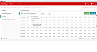
My program is working fine in debug mode. 

After building in Release mode, it also works fine with this option checked

But, if I am switching off/on my DSP, the program will not run.

I tried updating my Uniflash Software, as I saw in a forum but it didn't work.

I  hope I will find help, thank you very much.

Best Regards

Mattéo

  • Hi Mattéo,

    When you load and restart the device, are you able to see the flash maintain the program in the memory browser?

    Will get back to you within the next day.

    Thanks,

    Charles

  • Hello,

    I don't know how to see if the flash maintain the program in the memory.

    I tried to execute "Verify Image" in UniFlash, after making a on/off with the power supply, but I got "Target is not connected" error, even though the power supply is on.

    Thank you for your answer

    Mattéo 

  • Ok, I managed to check it with verify image, and I have this output, after pressing 

    [SUCCESS] C28xx: Program verification successful for //<file folder where my .out is>

    So I think the flash maintain the program ?

    Thank you again

    Mattéo

  • Hi Mattéo,

    A way to check if the flash maintains it's memory using Uniflash is to go to the Memory Tab once the device is connected and searching for the program location at the flash sectors.

    And yes, if it was able to verify the program that means it checked what was sent to the device. 

    If you are still encountering the program not running when switching off/on the DSP, then I would first check the Boot-to Flash Entry Point (address 0x33FF6 in memory). Also make sure the boot pins are set to Flash boot mode. 

    Let me know the update on this. 

    Thanks,

    Charles

  • Hello,

    Thank you for that clear answer, with all the screenshots

    On the Hardware side, all the GPIO of the Boot Mode are not connected, so because of the internal pullup, if I am not wrong, I am in Flash Mode I think.

    Then, on UniFlash, I have this in the Boot-to-Flash Entry Point after an on/off on my device :

    Where as, after being programmed ( I tried with the "Run Target After Program Load/Flash Operation" ceckbox checked, and unchecked, I have the same thing), I have this in my memory :

    Thank you again

    Best Regards

    Mattéo

  • I think it might help, so let me provide you my .cmd files :

    MEMORY
    {
    PAGE 0: /* Program Memory */
    /* Memory (RAM/FLASH/OTP) blocks can be moved to PAGE1 for data allocation */

    ZONE0 : origin = 0x004000, length = 0x001000 /* XINTF zone 0 */
    RAMFUNCS : origin = 0x008000, length = 0x003000 /* on-chip RAM block L0 to L2 */
    ZONE6 : origin = 0x100000, length = 0x100000 /* XINTF zone 6 */
    ZONE7A : origin = 0x200000, length = 0x00FC00 /* XINTF zone 7 - program space */
    BEGIN_FLASH_APPLI : origin = 0x3002FE, length = 0x000002 /* Part of FLASHH. Used for Watt booloader FLASH_APPLIcation entry point. */
    FLASH_APPLI : origin = 0x300300, length = 0x02FD00 /* Part of FLASHH, FLASHG, FLASHF, FLASHE, FLASHD, FLASHC used for application*/
    FLASHA : origin = 0x338000, length = 0x007F80 /* on-chip FLASHA, used for bootloader program */
    CSM_RSVD : origin = 0x33FF80, length = 0x000076 /* Part of FLASHA. Program with all 0x0000 when CSM is in use. */
    BEGIN : origin = 0x33FFF6, length = 0x000002 /* Part of FLASHA. Used for "boot to Flash" bootloader mode. */
    CSM_PWL : origin = 0x33FFF8, length = 0x000008 /* Part of FLASHA. CSM password locations in FLASHA */
    OTP : origin = 0x380400, length = 0x000400 /* on-chip OTP */
    ADC_CAL : origin = 0x380080, length = 0x000009 /* ADC_cal function in Reserved memory */

    //IQTABLES : origin = 0x3FE000, length = 0x000b50 /* IQ Math Tables in Boot ROM */
    //IQTABLES2 : origin = 0x3FEB50, length = 0x00008c /* IQ Math Tables in Boot ROM */
    FPUTABLES : origin = 0x3FEBDC, length = 0x0006A0 /* FPU Tables in Boot ROM */
    ROM : origin = 0x3FF27C, length = 0x000D44 /* Boot ROM */
    RESET : origin = 0x3FFFC0, length = 0x000002 /* part of boot ROM */
    VECTORS : origin = 0x3FFFC2, length = 0x00003E /* part of boot ROM */

    PAGE 1 : /* Data Memory */
    /* Memory (RAM/FLASH/OTP) blocks can be moved to PAGE0 for program allocation */
    /* Registers remain on PAGE1 */

    BOOT_RSVD : origin = 0x000000, length = 0x000050 /* Part of M0, BOOT rom will use this for stack */
    RAMM0 : origin = 0x000050, length = 0x0003B0 /* on-chip RAM block M0 */
    RAMM1 : origin = 0x000400, length = 0x000400 /* on-chip RAM block M1 */
    RAMM2 : origin = 0x002000, length = 0x001000 /* on-chip RAM block M2 */
    RAM_GLOBAL_VAR : origin = 0x00B000, length = 0x004B00 /* on-chip RAM block L3 to L6 and part of L7*/
    RAM_ADCRESULT : origin = 0x00FB00, length = 0x000400 /* on-chip RAM block last part of L7*/
    ZONE7B : origin = 0x20FC00, length = 0x000400 /* XINTF zone 7 - data space */
    FLASHB : origin = 0x330000, length = 0x008000 /* on-chip FLASH */
    }

    /* Allocate sections to memory blocks.
    Note:
    codestart user defined section in DSP28_CodeStartBranch.asm used to redirect code
    execution when booting to flash
    ramfuncs user defined section to store functions that will be copied from Flash into RAM
    */

    SECTIONS
    {

    /* Allocate program areas: */
    .cinit : > FLASH_APPLI PAGE = 0
    .pinit : > FLASH_APPLI, PAGE = 0
    .text : > FLASH_APPLI PAGE = 0
    codestart : > BEGIN_FLASH_APPLI PAGE = 0
    ramfuncs : LOAD = FLASH_APPLI,
    RUN = RAMFUNCS,/*RAML0,*/
    LOAD_START(_RamfuncsLoadStart),
    LOAD_END(_RamfuncsLoadEnd),
    RUN_START(_RamfuncsRunStart),
    PAGE = 0


    .FPUtables : LOAD = FLASH_APPLI
    RUN = RAMFUNCS,
    LOAD_START(_FPUtablesLoadStart),
    LOAD_END(_FPUtablesLoadEnd),
    RUN_START(_FPUtablesRunStart),
    PAGE = 0
    {
    -l rts2800_fpu32_fast_supplement.lib
    //-l rts2800_fpu32_fast_supplement_coff.lib
    }

    csmpasswds : > CSM_PWL PAGE = 0
    csm_rsvd : > CSM_RSVD PAGE = 0

    /* Allocate uninitalized data sections: */
    .stack : > RAMM1 PAGE = 1
    .ebss : > RAM_GLOBAL_VAR PAGE = 1
    .esysmem : > RAMM2 PAGE = 1
    .sysmem : > RAM_GLOBAL_VAR PAGE = 1

    /* Initalized sections go in Flash */
    /* For SDFlash to program these, they must be allocated to page 0 */
    .econst : > FLASH_APPLI PAGE = 0
    .switch : > FLASH_APPLI PAGE = 0

    /* Allocate IQ math areas: */
    //IQmath : > FLASH_APPLI PAGE = 0 /* Math Code */
    //IQmathTables : > IQTABLES, PAGE = 0, TYPE = NOLOAD

    /* Uncomment the section below if calling the IQNexp() or IQexp()
    functions from the IQMath.lib library in order to utilize the
    relevant IQ Math table in Boot ROM (This saves space and Boot ROM
    is 1 wait-state). If this section is not uncommented, IQmathTables2
    will be loaded into other memory (SARAM, Flash, etc.) and will take
    up space, but 0 wait-state is possible.
    */
    /*
    IQmathTables2 : > IQTABLES2, PAGE = 0, TYPE = NOLOAD
    {

    IQmath.lib<IQNexpTable.obj> (IQmathTablesRam)

    }
    */

    FPUmathTables : > FPUTABLES, PAGE = 0, TYPE = NOLOAD

    /* Allocate DMA-accessible RAM sections: */
    DMARAML4 : > RAM_ADCRESULT, PAGE = 1
    DMARAML5 : > RAM_ADCRESULT, PAGE = 1
    DMARAML6 : > RAM_ADCRESULT, PAGE = 1
    DMARAML7 : > RAM_ADCRESULT, PAGE = 1

    /* Allocate 0x400 of XINTF Zone 7 to storing data */
    ZONE7DATA : > ZONE7B, PAGE = 1

    /* .reset is a standard section used by the compiler. It contains the */
    /* the address of the start of _c_int00 for C Code. /*
    /* When using the boot ROM this section and the CPU vector */
    /* table is not needed. Thus the default type is set here to */
    /* DSECT */
    .reset : > RESET, PAGE = 0, TYPE = DSECT
    vectors : > VECTORS PAGE = 0, TYPE = DSECT

    /* Allocate ADC_cal function (pre-programmed by factory into TI reserved memory) */
    .adc_cal : load = ADC_CAL, PAGE = 0, TYPE = NOLOAD
    CRC16_TABLE : > RAM_GLOBAL_VAR PAGE = 1
    }
    /*

    MEMORY
    {
    PAGE 0: /* Program Memory */

    PAGE 1: /* Data Memory */

    DEV_EMU : origin = 0x000880, length = 0x000180 /* device emulation registers */
    FLASH_REGS : origin = 0x000A80, length = 0x000060 /* FLASH registers */
    CSM : origin = 0x000AE0, length = 0x000010 /* code security module registers */

    ADC_MIRROR : origin = 0x000B00, length = 0x000010 /* ADC Results register mirror */

    XINTF : origin = 0x000B20, length = 0x000020 /* external interface registers */

    CPU_TIMER0 : origin = 0x000C00, length = 0x000008 /* CPU Timer0 registers */
    CPU_TIMER1 : origin = 0x000C08, length = 0x000008 /* CPU Timer0 registers (CPU Timer1 & Timer2 reserved TI use)*/
    CPU_TIMER2 : origin = 0x000C10, length = 0x000008 /* CPU Timer0 registers (CPU Timer1 & Timer2 reserved TI use)*/

    PIE_CTRL : origin = 0x000CE0, length = 0x000020 /* PIE control registers */
    PIE_VECT : origin = 0x000D00, length = 0x000100 /* PIE Vector Table */

    DMA : origin = 0x001000, length = 0x000200 /* DMA registers */

    MCBSPA : origin = 0x005000, length = 0x000040 /* McBSP-A registers */
    MCBSPB : origin = 0x005040, length = 0x000040 /* McBSP-B registers */

    ECANA : origin = 0x006000, length = 0x000040 /* eCAN-A control and status registers */
    ECANA_LAM : origin = 0x006040, length = 0x000040 /* eCAN-A local acceptance masks */
    ECANA_MOTS : origin = 0x006080, length = 0x000040 /* eCAN-A message object time stamps */
    ECANA_MOTO : origin = 0x0060C0, length = 0x000040 /* eCAN-A object time-out registers */
    ECANA_MBOX : origin = 0x006100, length = 0x000100 /* eCAN-A mailboxes */

    ECANB : origin = 0x006200, length = 0x000040 /* eCAN-B control and status registers */
    ECANB_LAM : origin = 0x006240, length = 0x000040 /* eCAN-B local acceptance masks */
    ECANB_MOTS : origin = 0x006280, length = 0x000040 /* eCAN-B message object time stamps */
    ECANB_MOTO : origin = 0x0062C0, length = 0x000040 /* eCAN-B object time-out registers */
    ECANB_MBOX : origin = 0x006300, length = 0x000100 /* eCAN-B mailboxes */

    // EPWM1 : origin = 0x006800, length = 0x000022 /* Enhanced PWM 1 registers */
    // EPWM2 : origin = 0x006840, length = 0x000022 /* Enhanced PWM 2 registers */
    // EPWM3 : origin = 0x006880, length = 0x000022 /* Enhanced PWM 3 registers */
    // EPWM4 : origin = 0x0068C0, length = 0x000022 /* Enhanced PWM 4 registers */
    // EPWM5 : origin = 0x006900, length = 0x000022 /* Enhanced PWM 5 registers */
    // EPWM6 : origin = 0x006940, length = 0x000022 /* Enhanced PWM 6 registers */

    EPWM1 : origin = 0x005800, length = 0x000022 /* Enhanced PWM 1 registers */
    EPWM2 : origin = 0x005840, length = 0x000022 /* Enhanced PWM 2 registers */
    EPWM3 : origin = 0x005880, length = 0x000022 /* Enhanced PWM 3 registers */
    EPWM4 : origin = 0x0058C0, length = 0x000022 /* Enhanced PWM 4 registers */
    EPWM5 : origin = 0x005900, length = 0x000022 /* Enhanced PWM 5 registers */
    EPWM6 : origin = 0x005940, length = 0x000022 /* Enhanced PWM 6 registers */


    ECAP1 : origin = 0x006A00, length = 0x000020 /* Enhanced Capture 1 registers */
    ECAP2 : origin = 0x006A20, length = 0x000020 /* Enhanced Capture 2 registers */
    ECAP3 : origin = 0x006A40, length = 0x000020 /* Enhanced Capture 3 registers */
    ECAP4 : origin = 0x006A60, length = 0x000020 /* Enhanced Capture 4 registers */
    ECAP5 : origin = 0x006A80, length = 0x000020 /* Enhanced Capture 5 registers */
    ECAP6 : origin = 0x006AA0, length = 0x000020 /* Enhanced Capture 6 registers */

    EQEP1 : origin = 0x006B00, length = 0x000040 /* Enhanced QEP 1 registers */
    EQEP2 : origin = 0x006B40, length = 0x000040 /* Enhanced QEP 2 registers */

    GPIOCTRL : origin = 0x006F80, length = 0x000040 /* GPIO control registers */
    GPIODAT : origin = 0x006FC0, length = 0x000020 /* GPIO data registers */
    GPIOINT : origin = 0x006FE0, length = 0x000020 /* GPIO interrupt/LPM registers */

    SYSTEM : origin = 0x007010, length = 0x000020 /* System control registers */
    SPIA : origin = 0x007040, length = 0x000010 /* SPI-A registers */
    SCIA : origin = 0x007050, length = 0x000010 /* SCI-A registers */
    XINTRUPT : origin = 0x007070, length = 0x000010 /* external interrupt registers */

    ADC : origin = 0x007100, length = 0x000020 /* ADC registers */

    SCIB : origin = 0x007750, length = 0x000010 /* SCI-B registers */

    SCIC : origin = 0x007770, length = 0x000010 /* SCI-C registers */

    I2CA : origin = 0x007900, length = 0x000040 /* I2C-A registers */

    CSM_PWL : origin = 0x33FFF8, length = 0x000008 /* Part of FLASHA. CSM password locations. */

    PARTID : origin = 0x380090, length = 0x000001 /* Part ID register location */
    }


    SECTIONS
    {
    PieVectTableFile : > PIE_VECT, PAGE = 1

    /*** Peripheral Frame 0 Register Structures ***/
    DevEmuRegsFile : > DEV_EMU, PAGE = 1
    FlashRegsFile : > FLASH_REGS, PAGE = 1
    CsmRegsFile : > CSM, PAGE = 1
    AdcMirrorFile : > ADC_MIRROR, PAGE = 1
    XintfRegsFile : > XINTF, PAGE = 1
    CpuTimer0RegsFile : > CPU_TIMER0, PAGE = 1
    CpuTimer1RegsFile : > CPU_TIMER1, PAGE = 1
    CpuTimer2RegsFile : > CPU_TIMER2, PAGE = 1
    PieCtrlRegsFile : > PIE_CTRL, PAGE = 1
    DmaRegsFile : > DMA, PAGE = 1

    /*** Peripheral Frame 3 Register Structures ***/
    McbspaRegsFile : > MCBSPA, PAGE = 1
    McbspbRegsFile : > MCBSPB, PAGE = 1

    /*** Peripheral Frame 1 Register Structures ***/
    ECanaRegsFile : > ECANA, PAGE = 1
    ECanaLAMRegsFile : > ECANA_LAM PAGE = 1
    ECanaMboxesFile : > ECANA_MBOX PAGE = 1
    ECanaMOTSRegsFile : > ECANA_MOTS PAGE = 1
    ECanaMOTORegsFile : > ECANA_MOTO PAGE = 1

    ECanbRegsFile : > ECANB, PAGE = 1
    ECanbLAMRegsFile : > ECANB_LAM PAGE = 1
    ECanbMboxesFile : > ECANB_MBOX PAGE = 1
    ECanbMOTSRegsFile : > ECANB_MOTS PAGE = 1
    ECanbMOTORegsFile : > ECANB_MOTO PAGE = 1

    EPwm1RegsFile : > EPWM1 PAGE = 1
    EPwm2RegsFile : > EPWM2 PAGE = 1
    EPwm3RegsFile : > EPWM3 PAGE = 1
    EPwm4RegsFile : > EPWM4 PAGE = 1
    EPwm5RegsFile : > EPWM5 PAGE = 1
    EPwm6RegsFile : > EPWM6 PAGE = 1

    ECap1RegsFile : > ECAP1 PAGE = 1
    ECap2RegsFile : > ECAP2 PAGE = 1
    ECap3RegsFile : > ECAP3 PAGE = 1
    ECap4RegsFile : > ECAP4 PAGE = 1
    ECap5RegsFile : > ECAP5 PAGE = 1
    ECap6RegsFile : > ECAP6 PAGE = 1

    EQep1RegsFile : > EQEP1 PAGE = 1
    EQep2RegsFile : > EQEP2 PAGE = 1

    GpioCtrlRegsFile : > GPIOCTRL PAGE = 1
    GpioDataRegsFile : > GPIODAT PAGE = 1
    GpioIntRegsFile : > GPIOINT PAGE = 1

    /*** Peripheral Frame 2 Register Structures ***/
    SysCtrlRegsFile : > SYSTEM, PAGE = 1
    SpiaRegsFile : > SPIA, PAGE = 1
    SciaRegsFile : > SCIA, PAGE = 1
    XIntruptRegsFile : > XINTRUPT, PAGE = 1
    AdcRegsFile : > ADC, PAGE = 1
    ScibRegsFile : > SCIB, PAGE = 1
    ScicRegsFile : > SCIC, PAGE = 1
    I2caRegsFile : > I2CA, PAGE = 1

    /*** Code Security Module Register Structures ***/
    CsmPwlFile : > CSM_PWL, PAGE = 1

    /*** Device Part ID Register Structures ***/
    PartIdRegsFile : > PARTID, PAGE = 1

    }

    MEMORY
    {
    PAGE 0: /* Program Memory */

    UPGRADE_METADATA : origin = 0x300000, length = 0x000004 /* upgrade metadata registers */
    APPLICATION_METADATA : origin = 0x300004, length = 0x0002FA /* upgrade metadata registers */

    PAGE 1: /* Data Memory */


    }


    SECTIONS
    {
    UpgradeMetadataFile : > UPGRADE_METADATA , PAGE = 0
    ApplicationMetadataFile : > APPLICATION_METADATA, PAGE = 0

    SharedDataFile : > RAMM0 , PAGE = 1
    }

  • Ok, and last thing : 

    everything in my memory is "0BAD" when off/on the power of my DSP

    Best regards

    Mattéo

  • Mattéo,

    Is it possible you have a corruption within the PIE interrupt enable register?  If off/on connect results in 0BAD, but loading the program clears the memory, then I would check to see if the loading of the flash is getting interrupted. Also, I would check to seewhat the stack usage looks like. 

    Thanks and regards,

    Charles

  • Hi Mattéo,

    This is assigned to me today for review.  I will be able to review and get back to you by the end of the week.

    Thanks and regards,

    Vamsi

  • Hello,

    Thank you for taking care of my issue. 

    Let me show you the .cmd files I am using :

    /*
    // TI File $Revision: /main/8 $
    // Checkin $Date: June 2, 2008 11:12:24 $
    //###########################################################################
    //
    // FILE: DSP2833x_Headers_nonBIOS.cmd
    //
    // TITLE: DSP2833x Peripheral registers linker command file
    //
    // DESCRIPTION:
    //
    // This file is for use in Non-BIOS applications.
    //
    // Linker command file to place the peripheral structures
    // used within the DSP2833x headerfiles into the correct memory
    // mapped locations.
    //
    // This version of the file includes the PieVectorTable structure.
    // For BIOS applications, please use the DSP2833x_Headers_BIOS.cmd file
    // which does not include the PieVectorTable structure.
    //
    //###########################################################################
    */

    // Version History:
    //=============================================================================
    // Ver | dd mmm yyyy | Who | Description of changes
    // =====|=============|=======|================================================
    // 1.0 | 02 Jun 2008 | TI | Release Version
    // 2.0 | 06 Sep 2011 | WattC | ePWM mapping changed from 0x68xx to 0x58xx for DMA access
    //=============================================================================

    MEMORY
    {
    PAGE 0: /* Program Memory */

    PAGE 1: /* Data Memory */

    DEV_EMU : origin = 0x000880, length = 0x000180 /* device emulation registers */
    FLASH_REGS : origin = 0x000A80, length = 0x000060 /* FLASH registers */
    CSM : origin = 0x000AE0, length = 0x000010 /* code security module registers */

    ADC_MIRROR : origin = 0x000B00, length = 0x000010 /* ADC Results register mirror */

    XINTF : origin = 0x000B20, length = 0x000020 /* external interface registers */

    CPU_TIMER0 : origin = 0x000C00, length = 0x000008 /* CPU Timer0 registers */
    CPU_TIMER1 : origin = 0x000C08, length = 0x000008 /* CPU Timer0 registers (CPU Timer1 & Timer2 reserved TI use)*/
    CPU_TIMER2 : origin = 0x000C10, length = 0x000008 /* CPU Timer0 registers (CPU Timer1 & Timer2 reserved TI use)*/

    PIE_CTRL : origin = 0x000CE0, length = 0x000020 /* PIE control registers */
    PIE_VECT : origin = 0x000D00, length = 0x000100 /* PIE Vector Table */

    DMA : origin = 0x001000, length = 0x000200 /* DMA registers */

    MCBSPA : origin = 0x005000, length = 0x000040 /* McBSP-A registers */
    MCBSPB : origin = 0x005040, length = 0x000040 /* McBSP-B registers */

    ECANA : origin = 0x006000, length = 0x000040 /* eCAN-A control and status registers */
    ECANA_LAM : origin = 0x006040, length = 0x000040 /* eCAN-A local acceptance masks */
    ECANA_MOTS : origin = 0x006080, length = 0x000040 /* eCAN-A message object time stamps */
    ECANA_MOTO : origin = 0x0060C0, length = 0x000040 /* eCAN-A object time-out registers */
    ECANA_MBOX : origin = 0x006100, length = 0x000100 /* eCAN-A mailboxes */

    ECANB : origin = 0x006200, length = 0x000040 /* eCAN-B control and status registers */
    ECANB_LAM : origin = 0x006240, length = 0x000040 /* eCAN-B local acceptance masks */
    ECANB_MOTS : origin = 0x006280, length = 0x000040 /* eCAN-B message object time stamps */
    ECANB_MOTO : origin = 0x0062C0, length = 0x000040 /* eCAN-B object time-out registers */
    ECANB_MBOX : origin = 0x006300, length = 0x000100 /* eCAN-B mailboxes */

    // EPWM1 : origin = 0x006800, length = 0x000022 /* Enhanced PWM 1 registers */
    // EPWM2 : origin = 0x006840, length = 0x000022 /* Enhanced PWM 2 registers */
    // EPWM3 : origin = 0x006880, length = 0x000022 /* Enhanced PWM 3 registers */
    // EPWM4 : origin = 0x0068C0, length = 0x000022 /* Enhanced PWM 4 registers */
    // EPWM5 : origin = 0x006900, length = 0x000022 /* Enhanced PWM 5 registers */
    // EPWM6 : origin = 0x006940, length = 0x000022 /* Enhanced PWM 6 registers */

    EPWM1 : origin = 0x005800, length = 0x000022 /* Enhanced PWM 1 registers */
    EPWM2 : origin = 0x005840, length = 0x000022 /* Enhanced PWM 2 registers */
    EPWM3 : origin = 0x005880, length = 0x000022 /* Enhanced PWM 3 registers */
    EPWM4 : origin = 0x0058C0, length = 0x000022 /* Enhanced PWM 4 registers */
    EPWM5 : origin = 0x005900, length = 0x000022 /* Enhanced PWM 5 registers */
    EPWM6 : origin = 0x005940, length = 0x000022 /* Enhanced PWM 6 registers */


    ECAP1 : origin = 0x006A00, length = 0x000020 /* Enhanced Capture 1 registers */
    ECAP2 : origin = 0x006A20, length = 0x000020 /* Enhanced Capture 2 registers */
    ECAP3 : origin = 0x006A40, length = 0x000020 /* Enhanced Capture 3 registers */
    ECAP4 : origin = 0x006A60, length = 0x000020 /* Enhanced Capture 4 registers */
    ECAP5 : origin = 0x006A80, length = 0x000020 /* Enhanced Capture 5 registers */
    ECAP6 : origin = 0x006AA0, length = 0x000020 /* Enhanced Capture 6 registers */

    EQEP1 : origin = 0x006B00, length = 0x000040 /* Enhanced QEP 1 registers */
    EQEP2 : origin = 0x006B40, length = 0x000040 /* Enhanced QEP 2 registers */

    GPIOCTRL : origin = 0x006F80, length = 0x000040 /* GPIO control registers */
    GPIODAT : origin = 0x006FC0, length = 0x000020 /* GPIO data registers */
    GPIOINT : origin = 0x006FE0, length = 0x000020 /* GPIO interrupt/LPM registers */

    SYSTEM : origin = 0x007010, length = 0x000020 /* System control registers */
    SPIA : origin = 0x007040, length = 0x000010 /* SPI-A registers */
    SCIA : origin = 0x007050, length = 0x000010 /* SCI-A registers */
    XINTRUPT : origin = 0x007070, length = 0x000010 /* external interrupt registers */

    ADC : origin = 0x007100, length = 0x000020 /* ADC registers */

    SCIB : origin = 0x007750, length = 0x000010 /* SCI-B registers */

    SCIC : origin = 0x007770, length = 0x000010 /* SCI-C registers */

    I2CA : origin = 0x007900, length = 0x000040 /* I2C-A registers */

    CSM_PWL : origin = 0x33FFF8, length = 0x000008 /* Part of FLASHA. CSM password locations. */

    PARTID : origin = 0x380090, length = 0x000001 /* Part ID register location */
    }


    SECTIONS
    {
    PieVectTableFile : > PIE_VECT, PAGE = 1

    /*** Peripheral Frame 0 Register Structures ***/
    DevEmuRegsFile : > DEV_EMU, PAGE = 1
    FlashRegsFile : > FLASH_REGS, PAGE = 1
    CsmRegsFile : > CSM, PAGE = 1
    AdcMirrorFile : > ADC_MIRROR, PAGE = 1
    XintfRegsFile : > XINTF, PAGE = 1
    CpuTimer0RegsFile : > CPU_TIMER0, PAGE = 1
    CpuTimer1RegsFile : > CPU_TIMER1, PAGE = 1
    CpuTimer2RegsFile : > CPU_TIMER2, PAGE = 1
    PieCtrlRegsFile : > PIE_CTRL, PAGE = 1
    DmaRegsFile : > DMA, PAGE = 1

    /*** Peripheral Frame 3 Register Structures ***/
    McbspaRegsFile : > MCBSPA, PAGE = 1
    McbspbRegsFile : > MCBSPB, PAGE = 1

    /*** Peripheral Frame 1 Register Structures ***/
    ECanaRegsFile : > ECANA, PAGE = 1
    ECanaLAMRegsFile : > ECANA_LAM PAGE = 1
    ECanaMboxesFile : > ECANA_MBOX PAGE = 1
    ECanaMOTSRegsFile : > ECANA_MOTS PAGE = 1
    ECanaMOTORegsFile : > ECANA_MOTO PAGE = 1

    ECanbRegsFile : > ECANB, PAGE = 1
    ECanbLAMRegsFile : > ECANB_LAM PAGE = 1
    ECanbMboxesFile : > ECANB_MBOX PAGE = 1
    ECanbMOTSRegsFile : > ECANB_MOTS PAGE = 1
    ECanbMOTORegsFile : > ECANB_MOTO PAGE = 1

    EPwm1RegsFile : > EPWM1 PAGE = 1
    EPwm2RegsFile : > EPWM2 PAGE = 1
    EPwm3RegsFile : > EPWM3 PAGE = 1
    EPwm4RegsFile : > EPWM4 PAGE = 1
    EPwm5RegsFile : > EPWM5 PAGE = 1
    EPwm6RegsFile : > EPWM6 PAGE = 1

    ECap1RegsFile : > ECAP1 PAGE = 1
    ECap2RegsFile : > ECAP2 PAGE = 1
    ECap3RegsFile : > ECAP3 PAGE = 1
    ECap4RegsFile : > ECAP4 PAGE = 1
    ECap5RegsFile : > ECAP5 PAGE = 1
    ECap6RegsFile : > ECAP6 PAGE = 1

    EQep1RegsFile : > EQEP1 PAGE = 1
    EQep2RegsFile : > EQEP2 PAGE = 1

    GpioCtrlRegsFile : > GPIOCTRL PAGE = 1
    GpioDataRegsFile : > GPIODAT PAGE = 1
    GpioIntRegsFile : > GPIOINT PAGE = 1

    /*** Peripheral Frame 2 Register Structures ***/
    SysCtrlRegsFile : > SYSTEM, PAGE = 1
    SpiaRegsFile : > SPIA, PAGE = 1
    SciaRegsFile : > SCIA, PAGE = 1
    XIntruptRegsFile : > XINTRUPT, PAGE = 1
    AdcRegsFile : > ADC, PAGE = 1
    ScibRegsFile : > SCIB, PAGE = 1
    ScicRegsFile : > SCIC, PAGE = 1
    I2caRegsFile : > I2CA, PAGE = 1

    /*** Code Security Module Register Structures ***/
    CsmPwlFile : > CSM_PWL, PAGE = 1

    /*** Device Part ID Register Structures ***/
    PartIdRegsFile : > PARTID, PAGE = 1

    }


    /*
    //===========================================================================
    // End of file.
    //===========================================================================
    */

    /*
    //###########################################################################
    //
    // FILE: F28335.cmd
    //
    // TITLE: Linker Command File For F28335 Device
    //
    //###########################################################################
    // $TI Release: F2833x/F2823x Header Files and Peripheral Examples V140 $
    // $Release Date: March 4, 2015 $
    // $Copyright: Copyright (C) 2007-2015 Texas Instruments Incorporated -
    // http://www.ti.com/ ALL RIGHTS RESERVED $
    //###########################################################################
    */

    /* ======================================================
    // For Code Composer Studio V2.2 and later
    // ---------------------------------------
    // In addition to this memory linker command file,
    // add the header linker command file directly to the project.
    // The header linker command file is required to link the
    // peripheral structures to the proper locations within
    // the memory map.
    //
    // The header linker files are found in <base>\DSP2833x_Headers\cmd
    //
    // For BIOS applications add: DSP2833x_Headers_BIOS.cmd
    // For nonBIOS applications add: DSP2833x_Headers_nonBIOS.cmd
    ========================================================= */

    /* ======================================================
    // For Code Composer Studio prior to V2.2
    // --------------------------------------
    // 1) Use one of the following -l statements to include the
    // header linker command file in the project. The header linker
    // file is required to link the peripheral structures to the proper
    // locations within the memory map */

    /* Uncomment this line to include file only for non-BIOS applications */
    /* -l DSP2833x_Headers_nonBIOS.cmd */

    /* Uncomment this line to include file only for BIOS applications */
    /* -l DSP2833x_Headers_BIOS.cmd */

    /* 2) In your project add the path to <base>\DSP2833x_headers\cmd to the
    library search path under project->build options, linker tab,
    library search path (-i).
    /*========================================================= */

    /* Define the memory block start/length for the F28335
    PAGE 0 will be used to organize program sections
    PAGE 1 will be used to organize data sections

    Notes:
    Memory blocks on F28335 are uniform (ie same
    physical memory) in both PAGE 0 and PAGE 1.
    That is the same memory region should not be
    defined for both PAGE 0 and PAGE 1.
    Doing so will result in corruption of program
    and/or data.

    L0/L1/L2 and L3 memory blocks are mirrored - that is
    they can be accessed in high memory or low memory.
    For simplicity only one instance is used in this
    linker file.

    Contiguous SARAM memory blocks can be combined
    if required to create a larger memory block.
    */


    MEMORY
    {
    PAGE 0: /* Program Memory */
    /* Memory (RAM/FLASH/OTP) blocks can be moved to PAGE1 for data allocation */

    ZONE0 : origin = 0x004000, length = 0x001000 /* XINTF zone 0 */
    RAML0 : origin = 0x008000, length = 0x001000 /* on-chip RAM block L0 */
    RAML1 : origin = 0x009000, length = 0x001000 /* on-chip RAM block L1 */
    RAML2 : origin = 0x00A000, length = 0x001000 /* on-chip RAM block L2 */
    RAML3 : origin = 0x00B000, length = 0x001000 /* on-chip RAM block L3 */
    ZONE6 : origin = 0x0100000, length = 0x100000 /* XINTF zone 6 */
    ZONE7A : origin = 0x0200000, length = 0x00FC00 /* XINTF zone 7 - program space */
    // FLASHH : origin = 0x300000, length = 0x008000 /* on-chip FLASH */
    FLASHG : origin = 0x308000, length = 0x008000 /* on-chip FLASH */
    FLASHF : origin = 0x310000, length = 0x008000 /* on-chip FLASH */
    FLASHE : origin = 0x318000, length = 0x008000 /* on-chip FLASH */
    FLASHD : origin = 0x320000, length = 0x008000 /* on-chip FLASH */
    FLASHC : origin = 0x328000, length = 0x008000 /* on-chip FLASH */
    FLASHA : origin = 0x338000, length = 0x007F80 /* on-chip FLASH */
    CSM_RSVD : origin = 0x33FF80, length = 0x000076 /* Part of FLASHA. Program with all 0x0000 when CSM is in use. */
    BEGIN : origin = 0x33FFF6, length = 0x000002 /* Part of FLASHA. Used for "boot to Flash" bootloader mode. */
    CSM_PWL : origin = 0x33FFF8, length = 0x000008 /* Part of FLASHA. CSM password locations in FLASHA */
    OTP : origin = 0x380400, length = 0x000400 /* on-chip OTP */
    ADC_CAL : origin = 0x380080, length = 0x000009 /* ADC_cal function in Reserved memory */

    IQTABLES : origin = 0x3FE000, length = 0x000b50 /* IQ Math Tables in Boot ROM */
    IQTABLES2 : origin = 0x3FEB50, length = 0x00008c /* IQ Math Tables in Boot ROM */
    FPUTABLES : origin = 0x3FEBDC, length = 0x0006A0 /* FPU Tables in Boot ROM */
    ROM : origin = 0x3FF27C, length = 0x000D44 /* Boot ROM */
    RESET : origin = 0x3FFFC0, length = 0x000002 /* part of boot ROM */
    VECTORS : origin = 0x3FFFC2, length = 0x00003E /* part of boot ROM */

    PAGE 1 : /* Data Memory */
    /* Memory (RAM/FLASH/OTP) blocks can be moved to PAGE0 for program allocation */
    /* Registers remain on PAGE1 */

    BOOT_RSVD : origin = 0x000000, length = 0x000050 /* Part of M0, BOOT rom will use this for stack */
    RAMM0 : origin = 0x000050, length = 0x0003B0 /* on-chip RAM block M0 */
    RAMM1 : origin = 0x000400, length = 0x000400 /* on-chip RAM block M1 */
    RAML4 : origin = 0x00C000, length = 0x001000 /* on-chip RAM block L1 */
    RAML5 : origin = 0x00D000, length = 0x001000 /* on-chip RAM block L1 */
    RAML6 : origin = 0x00E000, length = 0x001000 /* on-chip RAM block L1 */
    RAML7 : origin = 0x00F000, length = 0x001000 /* on-chip RAM block L1 */
    ZONE7B : origin = 0x20FC00, length = 0x000400 /* XINTF zone 7 - data space */
    FLASHB : origin = 0x330000, length = 0x008000 /* on-chip FLASH */
    }

    /* Allocate sections to memory blocks.
    Note:
    codestart user defined section in DSP28_CodeStartBranch.asm used to redirect code
    execution when booting to flash
    ramfuncs user defined section to store functions that will be copied from Flash into RAM
    */

    SECTIONS
    {

    /* Allocate program areas: */
    .cinit : > FLASHA PAGE = 0
    .pinit : > FLASHA, PAGE = 0
    .text : > FLASHA PAGE = 0
    codestart : > BEGIN PAGE = 0
    ramfuncs : LOAD = FLASHD,
    RUN = RAML0,
    LOAD_START(_RamfuncsLoadStart),
    LOAD_END(_RamfuncsLoadEnd),
    RUN_START(_RamfuncsRunStart),
    LOAD_SIZE(_RamfuncsLoadSize),
    PAGE = 0

    csmpasswds : > CSM_PWL PAGE = 0
    csm_rsvd : > CSM_RSVD PAGE = 0

    /* Allocate uninitalized data sections: */
    .stack : > RAMM1 PAGE = 1
    .ebss : > RAML4 PAGE = 1
    .esysmem : > RAMM1 PAGE = 1

    /* Initalized sections go in Flash */
    /* For SDFlash to program these, they must be allocated to page 0 */
    .econst : > FLASHA PAGE = 0
    .switch : > FLASHA PAGE = 0

    /* Allocate IQ math areas: */
    IQmath : > FLASHC PAGE = 0 /* Math Code */
    IQmathTables : > IQTABLES, PAGE = 0, TYPE = NOLOAD

    /* Uncomment the section below if calling the IQNexp() or IQexp()
    functions from the IQMath.lib library in order to utilize the
    relevant IQ Math table in Boot ROM (This saves space and Boot ROM
    is 1 wait-state). If this section is not uncommented, IQmathTables2
    will be loaded into other memory (SARAM, Flash, etc.) and will take
    up space, but 0 wait-state is possible.
    */
    /*
    IQmathTables2 : > IQTABLES2, PAGE = 0, TYPE = NOLOAD
    {

    IQmath.lib<IQNexpTable.obj> (IQmathTablesRam)

    }
    */

    FPUmathTables : > FPUTABLES, PAGE = 0, TYPE = NOLOAD

    /* Allocate DMA-accessible RAM sections: */
    DMARAML4 : > RAML4, PAGE = 1
    DMARAML5 : > RAML5, PAGE = 1
    DMARAML6 : > RAML6, PAGE = 1
    DMARAML7 : > RAML7, PAGE = 1

    /* Allocate 0x400 of XINTF Zone 7 to storing data */
    ZONE7DATA : > ZONE7B, PAGE = 1

    /* .reset is a standard section used by the compiler. It contains the */
    /* the address of the start of _c_int00 for C Code. /*
    /* When using the boot ROM this section and the CPU vector */
    /* table is not needed. Thus the default type is set here to */
    /* DSECT */
    .reset : > RESET, PAGE = 0, TYPE = DSECT
    vectors : > VECTORS PAGE = 0, TYPE = DSECT

    /* Allocate ADC_cal function (pre-programmed by factory into TI reserved memory) */
    .adc_cal : load = ADC_CAL, PAGE = 0, TYPE = NOLOAD

    }

    /*
    //===========================================================================
    // End of file.
    //===========================================================================
    */


    /****************************************************************************
    *
    * Copyright (c) 2012 by Watt Consulting
    *
    * This software is copyrighted by and is the sole property of
    * Watt Consulting. All rights, title, ownership, or other interests
    * in the software remain the property of Watt Consulting. This
    * software may only be used in accordance with the corresponding
    * license agreement. Any unauthorized use, duplication, transmission,
    * distribution, or disclosure of this software is expressly forbidden.
    *
    * This Copyright notice may not be removed or modified without prior
    * written consent of Watt Consulting.
    *
    * Watt Consulting reserves the right to modify this software without notice.
    *
    * Watt Consulting
    * 23 rue Alexis de Tocqueville
    * 92160 Antony, FRANCE
    * contact@watt-consulting.com
    ****************************************************************************/

    /****************************************************************************
    *
    * CONFIDENTIAL NOTICE
    *
    * This document contains information confidential and proprietary to
    * Watt Consulting .The information may not be used, disclosed or reproduced
    * without the prior written authorization of Watt Consulting and those so
    * authorized may only use the information for the purpose of evaluation
    * consistent with authorization. Reproduction of any section of this document
    * must include this legend.
    ****************************************************************************/

    //=============================================================================
    ///
    /// @file MetadataHeader.cmd
    ///
    /// @brief Linker command file for metadata shared between Bootloader and Application
    ///
    /// @author Watt Consulting Team
    //=============================================================================

    MEMORY
    {
    PAGE 0: /* Program Memory */

    UPGRADE_METADATA : origin = 0x300000, length = 0x000004 /* upgrade metadata registers */
    APPLICATION_METADATA : origin = 0x300004, length = 0x0002FA /* upgrade metadata registers */

    PAGE 1: /* Data Memory */


    }


    SECTIONS
    {
    UpgradeMetadataFile : > UPGRADE_METADATA , PAGE = 0
    ApplicationMetadataFile : > APPLICATION_METADATA, PAGE = 0

    SharedDataFile : > RAMM0 , PAGE = 1
    }


    /*
    //===========================================================================
    // End of file.
    //===========================================================================
    */

  • Also, I look again how the memory is when I am looking after Off / On, and it looks like I have 0xFFFF in my memory, same value as before Off / On

  • Hello did you manage to take a look at this ?

    Best Regards

    Mattéo

  • Hi Mattéo,

    We asked our F28335 Flash expert to take a look at this.  He will get back to you in couple of days.

    Thanks and regards,
    Vamsi

  • Thank you very much for the update

    Best regards

    Mattéo

  • Mattéo,

    Would it be possible to connect to the target using CCS vs Uniflash to debug this using that IDE?

    What I would like to try there is the following:

    1)Connect to the target using CCS

    2)Load your .out file (this will have the same effect as Uniflash, invoking the Flash API and programming the device)

    3)Perform a "CPU Reset" under Run->Reset->CPU Reset

    4)Verify that the code is waiting at address 0x3F FFC0

    5)Run the code, halt, note where it is when halting.

    If with the above, the code is halted in your main code, then there is no reason standalone shouldn't work, but if it is not where it should be then this is also the reason the standalone didn't work before.

    We will need to go back and start debugging why the code isn't getting to main; but I'll let you try the above and see what happens at #5.

    Best,

    Matthew

  • Hello Matthew, 
    First of all, sorry for the delay, I had to work on other projects.
    Thank you for taking a look at this.

    I don't understand the first step "connect to the target using CCS". I didn't manage to find a "connect" button in CCS. Do you mean starting a debug session... ?

    Thank you for your answer

    Best Regards

    Mattéo Gerlin

  • Mattéo,

    I want to invoke the debug session, but in a slightly different way than the traditional debug session one click button.

    1)Open the target configuration window(Should be under View->Target configuration). 

    2)If you don't have a ccxml defined for your setup, go ahead and create one from scratch(right click in this window to start that process)

    3)If you have a ccxml there, right click on it and "launch debug session"

    4)This should pull up the debug view in CCS, and will show your target debug probe and then the C28x CPU underneath it.

    5)Right click on the C28x CPU and "connect target".  At this point you will be at step 1 in my previous post and can go from there.

    Reason to do the above and not the automatic/one click debug session, there are some background things that CCS does that I want to avoid happening to make the debug a bit more clear.

    Best,
    Matthew