This thread has been locked.

If you have a related question, please click the "Ask a related question" button in the top right corner. The newly created question will be automatically linked to this question.

LAUNCHXL-F28379D: Intermittent SPI Communication Errors with MAX1978

Part Number: LAUNCHXL-F28379D


Hello TI Community,

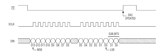
I am experiencing intermittent errors during SPI communication with a MAX1978 device. The communication works correctly for several cycles, sending and receiving the expected data (as shown by the initial correct 0x88 values in the waveform). However, occasionally the transmission is followed by errors where the expected data is not correctly received or sent (indicated by 'Error' in the waveform).

The errors are sporadic and do not follow a clear pattern. The waveform suggests that the issue may lie in the SPI configuration or signal integrity, but I've double-checked the settings, and they align with the device's requirements. The clock frequency, SPI mode, and bit order are configured according to the datasheet specifications, and the hardware connections have been verified.

Have any of you encountered similar issues or do you have insights into potential causes? Any suggestions for troubleshooting or specific areas to inspect would be greatly appreciated.

Thank you for your assistance.

Best regards, 

Nero Dai

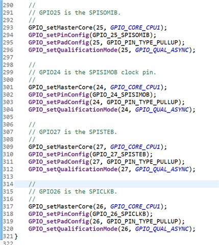
spi_ex3_external_loopback_fifo_interrupts.zipFull Code is here

  • Hi Nero,

    If you are receiving correct data at first, but then it seems to get corrupted there could be some timing or other configuration as you suspect. What is your SPICLK frequency and LSPCLK?

    Please also be sure that the SPI settings are meeting any specific timing requirements for MAX1978 as well as using the clock phase that MAX1978 is expecting. F2837xD SPI timing specifications can be found in the datasheet

    I assume the blue channel of that image is the chip select SPISTE line -does it always appear to spike high during the incorrect data transmissions? Or is it even transmissions without it going high that appear as incorrect? The chip select should remain low through the transmission.

    Best Regards,

    Allison

  • Hello Allison Nguyen,

    Thank you for your suggestions. I have indeed spent a considerable amount of time checking the clock polarity and phase, as discussed in my previous post (e2e.ti.com/.../launchxl-f28379d-max1978-not-responding-to-spi-dac-transmissions-from-c2000-mcu). Although I marked that thread as 'Resolved', the issue was not completely resolved.

    Regarding the CS signal, I agree it should be low during transmission, but I'm not sure how to maintain it low throughout the data transfer. In the spi_ex3_external_loopack_fifo_interrupts example, the __interrupt void spibTxFIFOISR(void) function initially had no DEVICE_DELAY_US(40); delay set. Without this delay, the CS signal wasn't even registering, which I've mentioned in my previous post.

    Could you guide me on how to ensure the CS signal stays low during the entire SPI transaction? Any insights on this would be greatly appreciated.

    Best regards,
    N

  • Hello Allison Nguyen,

    I am working towards achieving specific timing diagrams for SPI communication, and I have two reference timing charts that I need to match. I've been using the spi_ex3_external_loopback_fifo_interrupts example as a basis for my implementation. Given the timing requirements I have, do you think this example is a suitable starting point, or would you recommend a different example as a better fit for modification? Your guidance on selecting the most appropriate example to achieve these timing goals would be very helpful.

    Sincerely,
    N

  • void initSPIBMaster(void)
    {
        //
        // Must put SPI into reset before configuring it
        //
        SPI_disableModule(SPIB_BASE);
    
        //
        // SPI configuration. Use a 500kHz SPICLK and 16-bit word size.
        //
        SPI_setConfig(SPIB_BASE, DEVICE_LSPCLK_FREQ, SPI_PROT_POL0PHA0,
                      SPI_MODE_MASTER, 500000, 8);
        SPI_disableLoopback(SPIB_BASE);
        SPI_setEmulationMode(SPIB_BASE, SPI_EMULATION_FREE_RUN);
    //    SPI_setEmulationMode(SPIB_BASE, SPI_EMULATION_STOP_MIDWAY);
    
        //
        // FIFO and interrupt configuration
        //
        SPI_enableFIFO(SPIB_BASE);
        SPI_clearInterruptStatus(SPIB_BASE, SPI_INT_TXFF);
        SPI_setFIFOInterruptLevel(SPIB_BASE, SPI_FIFO_TX2, SPI_FIFO_RX2);
        SPI_enableInterrupt(SPIB_BASE, SPI_INT_TXFF);
    
        //
        // Configuration complete. Enable the module.
        //
        SPI_enableModule(SPIB_BASE);
    }

    __interrupt void spibTxFIFOISR(void)
    {
    // 计算DAC的固定值,例如0.3的比例
    uint16_t fixedData = (uint16_t)((0.2 / 1.5) * 65535); // 16-bit DAC value
    fixedData = fixedData << 2; // Left-justify the data to make it 16 bits

    // 将固定值放入sData数组中,准备发送
    sData[0] = fixedData;

    // 检查发送FIFO是否为空并准备好发送新数据
    while((SPI_getTxFIFOStatus(SPIB_BASE) & SPI_FIFO_TXEMPTY) != SPI_FIFO_TXEMPTY);

    // 发送数据
    SPI_writeDataNonBlocking(SPIB_BASE, sData[0]);
    // DEVICE_DELAY_US(40);

    // 清除发送FIFO中断标志
    SPI_clearInterruptStatus(SPIB_BASE, SPI_INT_TXFF);
    Interrupt_clearACKGroup(INTERRUPT_ACK_GROUP6);
    DEVICE_DELAY_US(100);
    }


  • Hi Nero,

    Thank you for all the information. Could you clarify if you are having issues with MAX1978 or MAX5144 specifically? The thread says 1978 but you circled 1544 so I want to be sure as I'm not familiar with these devices, only F2837xD. Can you also please explain the context of your system? i.e. what data are you trying to send/receive from which device and how many bits the data is.

    Here are some of my suggestions based on what you have provided:

    1. One thing you need to be sure of is that F2837xD SPI clock mode is set to match what the MAX device is expecting. From the diagrams of MAX device you attached, it looks like the MAX device is expecting a SPI clock that is idle-low and samples/latches data on the rising edge of SPICLK. So I would suggest using SPI mode 1 (polarity = 0, phase = 1).
    2. To ensure the chip select stays low during the entire communication, you could use a GPIO as your SPISTE chip select pin and manually control it (write a '0' to set it low just before communication and then write a '1' to set it back high after communication.
      1. A side-note: Some peripheral/slave devices operate in a manner where the chip select pin should be low continuously through multi-byte transmissions. If this is the case, and depending on what it is you are actually trying to do, you have a few options: (1) use a GPIO as your chip select SPISTE on F2837xD so you can manually set it low before communication and then manually set it back high after communication is completed. Or (2) you can send the desired number of bytes (transmit from F2837xD to MAX) all in a row first (to receive the same number of bytes from MAX) and once that is completed, only then would you read from the receive buffer all the bytes that F2837xD received. 
    3. From the other thread you linked, it looks like MAX operates in 8-bits only. F2837xD is optimized for 16 bits, so you need to be careful not to lose data here - this is dependent again on what you are trying to do/what type of data you are sending/receiving. In general, if sending 8-bit data from F2837xD, you should bit-shift left <<8 before writing to TXBUF. 8-bit data received b F2837xD should be aligned properly so no need to shift.
    4. Be sure you are meeting the timing requirements MAX is expecting. You can calculate what you have using the F2837xD data sheet section 8.12.5.1 SPI Electrical Data and Timing and compare to the MAX requirements to see if you are meeting them.

    Best Regards,

    Allison

  • Hi Allison,

    Thank you for the response. To clarify, the MAX5144 is a component on our MAX1978 evaluation board that we're using for SPI communication. It serves as the DAC being communicated with by our F2837xD MCU. We're aiming to accurately configure the SPI interface for correct data transmission to this DAC.

    Best,
    N


  • Hi Allison,

    Upon further analysis, using SPI mode 1 (polarity=0, phase=1) resulted in erroneous DAC values, which might stem from a misalignment between my implementation and the MAX5144's communication protocol. I resorted to (polarity=0, phase=0) because our senior hardware engineer successfully communicated with the DAC using these settings via a specialized SPI communication tester.

    For the CS control, I anticipated that the spi_ex3_external_loopback_fifo_interrupts example would automate CS toggling. Manually controlling CS seems counterintuitive when utilizing a standardized template. My experience with manual SPI register configuration is academic, so I'm navigating the practical application as a novice.

    Given the intricacies of timing requirements and SPI data handling, I foresee a week of iterative debugging to align with MAX5144's specifications. Immediate resolution might not be feasible as I calibrate the code to the device's precise operational cadence.

    Warm regards,
    N

  • Hi Nero,

    Thanks for the update. You are correct that the example automates chip select toggling. But I still suggested manually toggling it (writing it low before transmission and high after communication is complete) in order to see if the behavior/issue you see changes. Implementation shouldn't be too involved, so if you are able to test it, that would help us to know that this issue is unrelated to the chip select - you can do so by configuring SPISTE pin as a GPIO output pin, this way you have complete control over SPISTE pin via SW and can control when SPISTE pin is pulled low or high.

    Let me know if you are able to try this. Some other follow-up questions: how many bytes of data are you trying to send/receive in your application and is there any pattern in which bytes of data are erroneous?

    Best Regards,

    Allison

  • Hi Allison,

    I'm quite new to this work and still familiarizing myself with many of the settings. To add to the challenge, our senior software engineer is currently on vacation, so I'm navigating these issues mostly on my own. I've been working on manually controlling the chip select (CS) signal for the SPI communication. Based on your suggestion, I've reconfigured GPIO27, originally set as SPISTEB, to a general-purpose output pin for manual CS control. I've modified the spibTxFIFOISR function to set GPIO27 low before transmission and high afterwards. Here's the code snippet I'm working with:

    // Reconfigure GPIO27 as general-purpose output
    GPIO_setPinConfig(GPIO_27_GPIO27);
    GPIO_setDirectionMode(27, GPIO_DIR_MODE_OUT);
    
    __interrupt void spibTxFIFOISR(void) {
        GPIO_writePin(27, 0); // Set CS low before transmission
        // Data transmission code...
        GPIO_writePin(27, 1); // Set CS high after transmission
    }
    

    Thank you for your continued support. Any further guidance would be greatly appreciated.

    Best, 

    N

  • Hi Nero,

    Yes, your understanding of how to implement GPIO chip select looks correct (just be cautious of writing the chip select high too soon before transmission is complete in FIFO mode - you can just check that the TX FIFO is empty before writing chip select high). Please let me know if you see different behavior using this or have other updates on your progress.

    Best Regards,

    Allison

  • Hi Allison,

    After configuring the manual toggling of CS, our signal output has become incorrect. I’ve attached an oscilloscope screenshot showing the current signal pattern. As you can see, the CS line behavior has significantly changed, and it seems to be disrupting the data transmission. I followed the guidelines to set GPIO27 low before transmission and high afterwards, but this has led to unexpected results. Could you advise on potential missteps in this process or suggest what could be causing this new issue?

    Full source code 

    Best regards, 

    N

  • still wrong lol

  • Hi Nero,

    Just want to clarify is the green signal in these images the MOSI line, not MISO?

    Some important things to check when using SPI FIFO mode if you are controlling the chip select pin manually::

    1. You should always check that the transmit FIFO has space before writing to it to transmit your data 
    2. Be sure you write '0' to the GPIO right before transmission 
    3. Be sure you check that all data has been successfully/completely transmitted before writing '1' to the GPIO to bring it high again

    Items 1. and 2. above look ok, but it does not look like you are doing item 3. in your program right now. Keep in mind that writing data to TXBUF happens faster than data is actually sent out of the transmit FIFO to the other device. You need to add a line of code to check that the TXFFST bit (the Transmit FIFO Status bit) is 0 (meaning the transmit FIFO is empty and data has actually been sent out) before your line of code that writes a '1' to the GPIO27. This could be a simple while loop (e.g. while (SpiaRegs.SPIFFTX.RXFFST != 0)=;)

    Best Regards,

    Allison