This thread has been locked.
If you have a related question, please click the "Ask a related question" button in the top right corner. The newly created question will be automatically linked to this question.
I am starting to implement an emulation EEPROM (Fee) on TMS320F28388D and I only found this thread as a support material.
I am planning to start from the example which is included in HALCoGen tool (http://www.ti.com/tool/HALCOGEN) for the device “TMS570LS31x_21x” (\ti\Hercules\HALCoGen\v04.07.01\examples\TMS570LS31x_21x\example_TI_Fee_Write_Read)
Is it the right starting path ?
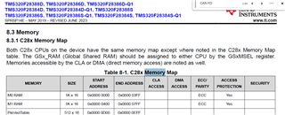
Another problem is I can not find the memory layout in the user-manual, do you have guidelines where to find it?
H Ahmed,
We now have an example for a C2000 device. Please take a look at https://e2e.ti.com/support/microcontrollers/c2000-microcontrollers-group/c2000/f/c2000-microcontrollers-forum/1301228/tms320f28379d-eeprom-emulation
Thanks and regards,
Vamsi
I see in the example (C:\ti\c2000\C2000Ware_5_01_00_00\driverlib\f28p65x\examples\c28x\flash) there is no memmap meanwhile you are trying to load some sections from Flash into Ram
My question is how you manage to pick only these sections for coping or you just copy all the .text from the FLASH_BANK0 into RAMD0 ?!
.TI.ramfunc : LOAD = FLASH_BANK0, RUN = RAMD0, // Can run in RAM for optimal cycle performance LOAD_START(RamfuncsLoadStart), LOAD_SIZE(RamfuncsLoadSize), LOAD_END(RamfuncsLoadEnd), RUN_START(RamfuncsRunStart), RUN_SIZE(RamfuncsRunSize), RUN_END(RamfuncsRunEnd), ALIGN(8)
Also I am using TMS320F28388D which means I have a single bank per each CPU, so:
Sectors | |||
Sector0 | 8Kx16 | 0x00080000 | 0x00081FFF |
Sector1 | 8Kx16 | 0x00082000 | 0x00083FFF |
Sector2 | 8Kx16 | 0x00084000 | 0x00085FFF |
Sector3 | 8Kx16 | 0x00086000 | 0x00087FFF |
Sector4 | 32Kx16 | 0x00088000 | 0x0008FFFF |
Sector5 | 32Kx16 | 0x00090000 | 0x00097FFF |
Sector6 | 32Kx16 | 0x00098000 | 0x0009FFFF |
Sector7 | 32Kx16 | 0x000A0000 | 0x000A7FFF |
Sector8 | 32Kx16 | 0x000A8000 | 0x000AFFFF |
Sector9 | 32Kx16 | 0x000B0000 | 0x000B7FFF |
Sector10 | 8Kx16 | 0x000B8000 | 0x000B9FFF |
Sector11 | 8Kx16 | 0x000BA000 | 0x000BBFFF |
Sector12 | 8Kx16 | 0x000BC000 | 0x000BDFFF |
Sector13 | 8Kx16 | 0x000BE000 | 0x000BFFFF |
Hi Ahmed,
1) Could you explain what you mean by memmap not available in the example? Do you mean to ask how different sections of the application are mapped to different memory ranges? If yes, it would be in the linker command file as you know.
2) Regarding selecting the sections for RAM execution instead of flash execution: There are two kinds of code that needs to run from RAM.
First is the configuration code/time-sensitive code that needs to be run from RAM (load to RAM but copy to RAM for execution) - Examples: (i) Flash should be configured only by the code executing from RAM. (ii) A delay function that is characterized to provide configurable delay.
Second is the performance-critical code: User applications may have performance-critical code that is best when run from 0-waitstate RAM instead of >0 waitstate Flash.
3) Each CPU has a dedicated 512KB bank.
4) Emulation sectors: You can decide this based on what your application needs and how your application is designed. If CPU1 has the data that needs to be stored in flash (as an EEPROM), then you can allocate couple of sectors in CPU1 flash bank. Or, if you have some performance-critical tight control loops on CPU1, you may decide to instead consider CPU2 to store the data in it's flash bank (if that is ok for your application).
5) Flash memory map per CPU: Each CPU has it's dedicated flash bank - however, the addresses are not unique between the CPUs. CPU1 has it's dedicated flash bank starting at CPU1's 0x80000 address. And, CPU2 has it's dedicated flash bank starting at CPU2's 0x80000 address.
6) As we mentioned in Table 7-5 Flash wait states of the datasheet, flash needs 3 wait-states at 200MHz.
7) It might be redundant from the fact that the flash_programming_f28p65x.h is actually copied from the flash programming example for other defines. I will ask our team to confirm this for you.
Thanks and regards,
Vamsi