Other Parts Discussed in Thread: TMDSCNCD28388D
Hi,
I've been using the TMDSCNCD28388D daughter board to communicate with SPI devices. The comms settings are as follows:
- Data width: 8 bits
- Bit rate: 1Mbps
- Mode: controller
Everything works fine with Rising Edge clocking schemes (Cpol = 0).
However, on the falling edge schemes (Cpol = 1, Cpha = 0 or 1), I am seeing an abnormal behaviour on the clock line.
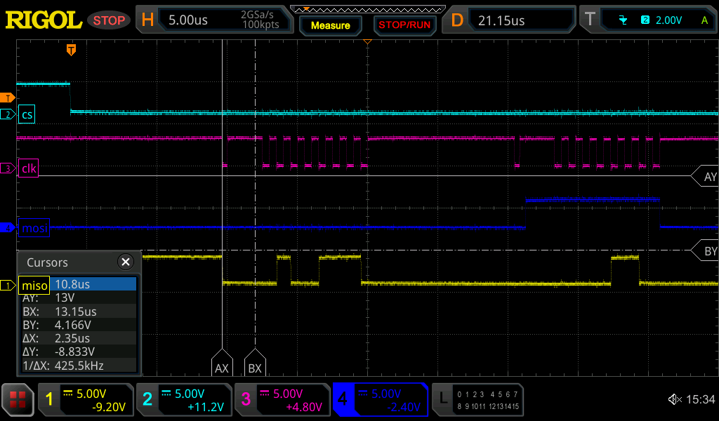
Here are some waveforms:
1. Rising edge scheme (Cpol = 0)

2. Falling edge scheme (Cpol = 1)

As shown in the above wave forms, the rising edge schemes have exactly 8 clock pulses for 8 bits. However, for some reasons, the falling edge schemes have an additional pulse. Because of this extra clock pulse (which looks like a spurious pulse), the data (in/out) will be wrong. For example, the MOSI data is supposed to be 0xFF, but is latched as 0x3F, due to the extra pulses (before and after the normal 8 pulses).
I've tried with all of the SPI modules (SPIA,B,C,D), and use different clock pins, but still facing the same issue.
My configuration code is similar to the spi_ex6_eeprom example project (except I'm using SPI_PROT_POL1PHA0 or SPI_PROT_POL0PHA1).
void mySPI0_init(){
SPI_disableModule(mySPI0_BASE);
SPI_setConfig(mySPI0_BASE, DEVICE_LSPCLK_FREQ, SPI_PROT_POL1PHA0,
SPI_MODE_CONTROLLER, 1000000, 8);
SPI_setPTESignalPolarity(mySPI0_BASE, SPI_PTE_ACTIVE_LOW);
SPI_disableFIFO(mySPI0_BASE);
SPI_disableLoopback(mySPI0_BASE);
SPI_setEmulationMode(mySPI0_BASE, SPI_EMULATION_STOP_MIDWAY);
SPI_enableModule(mySPI0_BASE);
}
void PinMux_init()
{
GPIO_setPinConfig(GPIO_11_GPIO11);
GPIO_setPinConfig(mySPI0_SPIPICO_PIN_CONFIG);
GPIO_setPadConfig(mySPI0_SPIPICO_GPIO, GPIO_PIN_TYPE_STD);
GPIO_setQualificationMode(mySPI0_SPIPICO_GPIO, GPIO_QUAL_ASYNC);
GPIO_setPinConfig(mySPI0_SPIPOCI_PIN_CONFIG);
GPIO_setPadConfig(mySPI0_SPIPOCI_GPIO, GPIO_PIN_TYPE_STD);
GPIO_setQualificationMode(mySPI0_SPIPOCI_GPIO, GPIO_QUAL_ASYNC);
GPIO_setPinConfig(mySPI0_SPICLK_PIN_CONFIG);
GPIO_setPadConfig(mySPI0_SPICLK_GPIO, GPIO_PIN_TYPE_STD);
GPIO_setQualificationMode(mySPI0_SPICLK_GPIO, GPIO_QUAL_ASYNC);
}
Please let me know if I miss anything to make the clock work properly in the falling edge schemes.
Thanks very much,
Regards,