This thread has been locked.

If you have a related question, please click the "Ask a related question" button in the top right corner. The newly created question will be automatically linked to this question.

TMS320F280037C: Proper Flash Write Flow

Part Number: TMS320F280037C
Other Parts Discussed in Thread: SYSBIOS

Hello,

I am developping a flash manager that will write some important data like test results and the Node ID for a CAN network. I am wondering how should addres this in terms of flash addres management.

For now, the variables that will be saved are a test result that should be run once in a lifetime and the Value of the Node ID that may change several time on its lifetime. I came accros three questions that i would like to share with you.

First, regarding that I only want to erase a part of the sector to write new data, I would like to know if there is a better way of writting the flash in comparison to saving the sector to be erased in another sector, erase and copy the contents with the new data. Second, I would like to know if the functions that will call the flash api will also be needed to be put in RAM or I can leave them in FLASH as soon as the Sector to be erased does not contain the code execution. Finally, I would like to know if the best practice is to reserve a sector to be filled with these kind of variables or they should be scattered in different sectors or even be put in the same sectors where code is running.

Regards,

David

  • Hi David,

    The minimum erasable unit in the flash bank on this device is a sector - It is not possible to erase only a part of the sector.

    When you say you want to know if there is a better way of writing the flash:  What is the size of the data that you plan to write in to the sector?  Will that occupy the entire sector?  If not, you can program multiple such data entries in to the sector until it gets full and then switch that data to a new sector so that you can erase the previously filled sector.  Which means, you don't have to erase the sector each time you want to update the data.  We do have a EEPROM emulation example available for TMS320F28P65x - https://www.ti.com/lit/pdf/sprade8.  Also, we plan to release F28003x based EEPROM example in March.  

    Flash API can be executed from one flash bank while you program/erase another flash bank (please consider this errata though: https://e2e.ti.com/support/microcontrollers/c2000-microcontrollers-group/c2000/f/c2000-microcontrollers-forum/1320238/faq-tms320f280039x-tms320f28004x-flash-api-usage-advisory-errata).  However, you can't execute the flash API from the same flash bank on which you plan to do erase/program operations for data storing.

    Best practice would be to reserve couple of sectors and start filling in one sector and switch to other sector when the first sector is full.

    Thanks and regards,
    Vamsi

  • Hello Vamsi,

    The size of the data for now would be variables of 32 bit so for now the sector is too big for our needs. Also, is did not undestand this part:

    f not, you can program multiple such data entries in to the sector until it gets full and then switch that data to a new sector so that you can erase the previously filled sector.

    You mean to program the entire flash sector with the same variables until the sector is occupied? Why would it be better this oslution than just programming the variables once?

    After reading the application note, I am afraisd I still do not undestand this approach. The point of having an EEPROM emulation would be that I can can be wiritng several instances of the same variable in different flash addresses each time a value update is requested? Then should I read the last value found in the EEPROM as the actual value?

    Regards,

    David

  • Also, I have another question about the linker file .cmd. What happen if two different code sections are in assigned to the same lfash bank? I there any problem about that?

  • Hi David,

    I can review and get back to you in a day or two.

    Thanks and regards,
    Vamsi

  • Hello Vamsi,

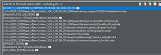
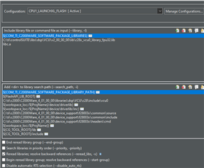
    Thank you for your help. Also, would it be possible to take a look at this error i get when i try to integrate the libraries into our prject?

    The error appears in a file that is from the c2000 installation, i do not know how it is posible to obtain that error. I get these errors when i include the file F021_F28003x_C28x.h.

    The .cmd i am using is the following:

    MEMORY
    {
       BEGIN               : origin = 0x00080000, length = 0x00000002
       BOOT_RSVD        : origin = 0x00000002, length = 0x00000126

       RAMM0               : origin = 0x00000128, length = 0x000002D8
       RAMM1            : origin = 0x00000400, length = 0x00000380     /* on-chip RAM block M1 */
       BOOT_RSVD_SYSBIOS: origin = 0x00000780, length = 0x00000080

    /* RAMLS0           : origin = 0x00008000, length = 0x00000800
       RAMLS1           : origin = 0x00008800, length = 0x00000800
       RAMLS2           : origin = 0x00009000, length = 0x00000800
       RAMLS3           : origin = 0x00009800, length = 0x00000800
       RAMLS4           : origin = 0x0000A000, length = 0x00000800 */
       RAMLS04          : origin = 0x00008000, length = 0x00002800
       RAMLS5           : origin = 0x0000A800, length = 0x00000800
       RAMLS6           : origin = 0x0000B000, length = 0x00000800
       RAMLS7           : origin = 0x0000B800, length = 0x00000800
       
       RAMGS0           : origin = 0x0000C000, length = 0x00001000
       RAMGS1           : origin = 0x0000D000, length = 0x00001000
       RAMGS2           : origin = 0x0000E000, length = 0x00001000
       RAMGS3           : origin = 0x0000F000, length = 0x00001000

       BOOTROM          : origin = 0x003F8000, length = 0x00007FC0
       SECURE_ROM       : origin = 0x003F2000, length = 0x00006000

       RESET            : origin = 0x003FFFC0, length = 0x00000002

       /* Flash sectors */
       /* BANK 0 */
       FLASH_BANK0_SEC0  : origin = 0x080002, length = 0x000FFE
       FLASH_BANK0_SEC1  : origin = 0x081000, length = 0x001000
       FLASH_BANK0_SEC2  : origin = 0x082000, length = 0x001000
       FLASH_BANK0_SEC3  : origin = 0x083000, length = 0x001000
       FLASH_BANK0_SEC4  : origin = 0x084000, length = 0x001000
       FLASH_BANK0_SEC5  : origin = 0x085000, length = 0x001000
       FLASH_BANK0_SEC6  : origin = 0x086000, length = 0x001000
       FLASH_BANK0_SEC7  : origin = 0x087000, length = 0x001000
       FLASH_BANK0_SEC8  : origin = 0x088000, length = 0x001000
       FLASH_BANK0_SEC9  : origin = 0x089000, length = 0x001000
       FLASH_BANK0_SEC10 : origin = 0x08A000, length = 0x001000
       FLASH_BANK0_SEC11 : origin = 0x08B000, length = 0x001000
       FLASH_BANK0_SEC12 : origin = 0x08C000, length = 0x001000
       FLASH_BANK0_SEC13 : origin = 0x08D000, length = 0x001000
       FLASH_BANK0_SEC14 : origin = 0x08E000, length = 0x001000
       FLASH_BANK0_SEC15 : origin = 0x08F000, length = 0x001000

       /* BANK 1 */
       FLASH_BANK1_SEC0  : origin = 0x090000, length = 0x001000
       FLASH_BANK1_SEC1  : origin = 0x091000, length = 0x001000
       FLASH_BANK1_SEC2  : origin = 0x092000, length = 0x001000
       FLASH_BANK1_SEC3  : origin = 0x093000, length = 0x001000
       FLASH_BANK1_SEC4  : origin = 0x094000, length = 0x001000
       FLASH_BANK1_SEC5_6  : origin = 0x095000, length = 0x002000
       //FLASH_BANK1_SEC5  : origin = 0x095000, length = 0x001000
       //FLASH_BANK1_SEC6  : origin = 0x096000, length = 0x001000
       FLASH_BANK1_SEC7  : origin = 0x097000, length = 0x001000
       FLASH_BANK1_SEC8  : origin = 0x098000, length = 0x001000
       FLASH_BANK1_SEC9  : origin = 0x099000, length = 0x001000
       FLASH_BANK1_SEC10 : origin = 0x09A000, length = 0x001000
       FLASH_BANK1_SEC11 : origin = 0x09B000, length = 0x001000
       FLASH_BANK1_SEC12 : origin = 0x09C000, length = 0x001000
       FLASH_BANK1_SEC13 : origin = 0x09D000, length = 0x001000
       FLASH_BANK1_SEC14 : origin = 0x09E000, length = 0x001000
       FLASH_BANK1_SEC15 : origin = 0x09F000, length = 0x001000

      /* BANK 2 */
       FLASH_BANK2_SEC0  : origin = 0x0A0000, length = 0x001000
       FLASH_BANK2_SEC1  : origin = 0x0A1000, length = 0x001000
       FLASH_BANK2_SEC2  : origin = 0x0A2000, length = 0x001000
       FLASH_BANK2_SEC3  : origin = 0x0A3000, length = 0x001000
       FLASH_BANK2_SEC4  : origin = 0x0A4000, length = 0x001000
       FLASH_BANK2_SEC5  : origin = 0x0A5000, length = 0x001000
       FLASH_BANK2_SEC6  : origin = 0x0A6000, length = 0x001000
       FLASH_BANK2_SEC7  : origin = 0x0A7000, length = 0x001000
       FLASH_BANK2_SEC8  : origin = 0x0A8000, length = 0x001000
       FLASH_BANK2_SEC9  : origin = 0x0A9000, length = 0x001000
       FLASH_BANK2_SEC10 : origin = 0x0AA000, length = 0x001000
       FLASH_BANK2_SEC11 : origin = 0x0AB000, length = 0x001000
       FLASH_BANK2_SEC12 : origin = 0x0AC000, length = 0x001000
       FLASH_BANK2_SEC13 : origin = 0x0AD000, length = 0x001000
       FLASH_BANK2_SEC14 : origin = 0x0AE000, length = 0x001000
       FLASH_BANK2_SEC15 : origin = 0x0AF000, length = 0x001000


    }


    SECTIONS
    {
       codestart        : > BEGIN, ALIGN(8)
       .text            : >> FLASH_BANK0_SEC2 | FLASH_BANK0_SEC3 | FLASH_BANK0_SEC4 | FLASH_BANK0_SEC5 | FLASH_BANK0_SEC6 | FLASH_BANK0_SEC7 | FLASH_BANK0_SEC8,   ALIGN(8)
       .cinit           : > FLASH_BANK0_SEC1,  ALIGN(8)
       .switch          : > FLASH_BANK0_SEC1,  ALIGN(8)
       .reset           : > RESET,                  TYPE = DSECT /* not used, */

       .stack           : > RAMM1

    #if defined(__TI_EABI__)
       .init_array      : > FLASH_BANK0_SEC1,  ALIGN(8)
       .bss             : > RAMLS5
       .bss:output      : > RAMLS04
       .bss:cio         : > RAMLS04
       .data            : > RAMLS5
       .sysmem          : > RAMLS5
       .const           : > FLASH_BANK1_SEC5_6,  ALIGN(8)
    #else
       .pinit           : > FLASH_BANK0_SEC1,  ALIGN(8)
       .ebss            : >> RAMLS5 | RAMLS6
       .esysmem         : > RAMLS5
       .cio             : > RAMLS04
       .econst          : > FLASH_BANK0_SEC9,  ALIGN(8)
    #endif

        ramgs0 : > RAMGS0
        ramgs1 : > RAMGS0

        /*  Allocate IQ math areas: */
       IQmath           : > FLASH_BANK0_SEC1, ALIGN(8)
       IQmathTables     : > FLASH_BANK0_SEC2, ALIGN(8)

     GROUP
       {
           .TI.ramfunc
           { -l FAPI_F28003x_COFF_v1.58.01.lib}

       }  LOAD = FLASH_BANK0_SEC1,
          RUN = RAMLS04,
          LOAD_START(_RamfuncsLoadStart),
          LOAD_SIZE(_RamfuncsLoadSize),
          LOAD_END(_RamfuncsLoadEnd),
          RUN_START(_RamfuncsRunStart),
          RUN_SIZE(_RamfuncsRunSize),
          RUN_END(_RamfuncsRunEnd),
          ALIGN(8)

        /*  TBD las variables que se usaran */

        DataBufferSection : > RAMM1, ALIGN(8)

    }

    Finally, the include options of linker and files:

  • Hi David,

    Please open new posts for each of your new questions - this will help our team to support you well.  We can discuss the original question in this thread.

    Thanks and regards,
    Vamsi

  • David,

    Regarding your questions on the EEPROM model that I suggested: 

    • 1) You don't need to program the same variable through out the sector.  You would start at the first location of the sector to program the first value of the chosen variable.  Whenever you have an updated value that you want to program, you would program it in the next available address.  And you continue until the sector (EEPROM banks/pages) are full.
    • 2) Yes, you would read the last programmed data.  There is a function in the EEPROM driver that you can use to read the last programmed data. Please read through the guide and let us know if you have any specific questions.  

    Regarding the code section mapping to flash bank: There is no any problem in mapping two different code sections to a given Flash entry in the linker command file.  Linker will not allocate both sections at the same address in the flash bank.  Linker will allocate different address ranges for those code sections.  You can review the map file after you compile to know where linker placed each of those sections.

    Thanks and regards,

    Vamsi

  • Hello Vamsi,

    Thank for your response. I understood the behavior. For now, I will try to implement the EEPROM emulation. Thank your very much for your help.

    Regards,

    David