This thread has been locked.

If you have a related question, please click the "Ask a related question" button in the top right corner. The newly created question will be automatically linked to this question.

TMS320F28388D: SPI between TMDSCNCD28388D and MB4

Part Number: TMS320F28388D
Other Parts Discussed in Thread: SYSCONFIG, C2000WARE

Tool/software:

Hi,

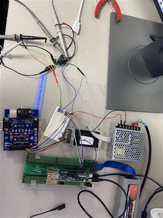
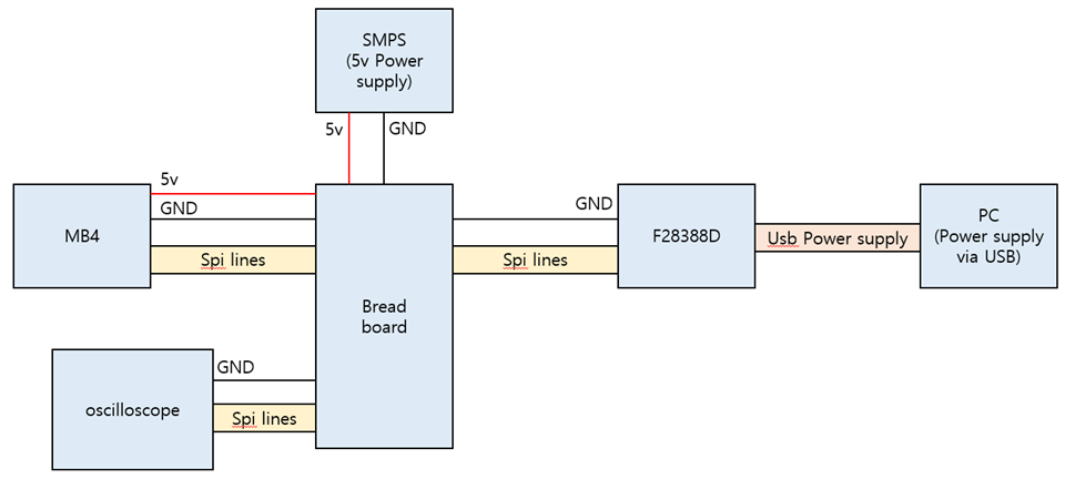
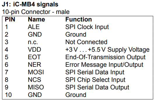
I'm trying SPI communication between TMS320F28388D and MB4 iC. TMS320F28388D works as SPI master, and MB4 works as SPI slave.
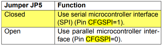
The picture below is the MB4 SPI protocol and the OP codes for Register READ/WRITE from the iC MB4 datasheet.
(iC MB4 datasheet download link : https://www.ichaus.de/product/ic-mb4/#documents)
  

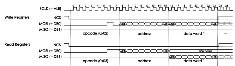
This is the information on the register I want to access to.

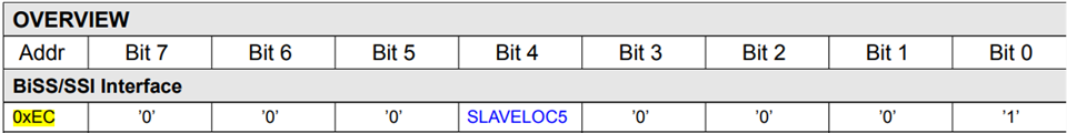
I want to set SLAVELOC5 to 1, so I tried writing 0x10 to the Register with the address 0xEC.

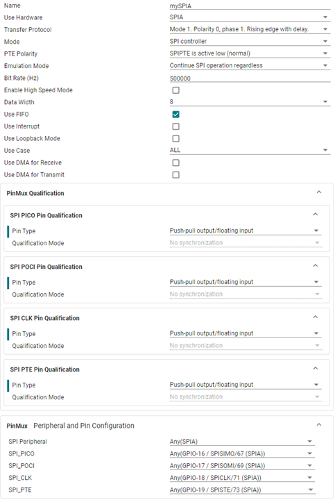
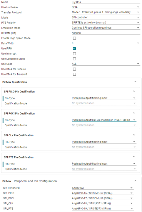
I set the sysconfig and wrote a code to make this SPI protocol. What I did was write 0x10 to the register, and then read the register value.

/*Included Files*/
#include "driverlib.h"
#include "device.h"
#include "board.h"
#include <stdio.h>


//OP CODE
#define WR_REG                      0x02
#define RD_REG                      0x03
#define RD_STS                      0x05
#define WR_INS                      0x07

//Register Addr
#define SLAVELOC5                   0xEC


/*private code*/
#define nData                       3
uint16_t TxData[nData] = {0,};
uint16_t RxData[nData] = {0,};
uint32_t txData = 0;
uint16_t txDelay = 0;


/*Main*/
void main(void)
{
    /*start settings*/
    // Initialize device clock and peripherals
    Device_init();

    // Disable pin locks and enable internal pullups.
    Device_initGPIO();

    // Initialize PIE and clear PIE registers. Disables CPU interrupts.
    Interrupt_initModule();

    // Initialize the PIE vector table with pointers to the shell Interrupt
    // Service Routines (ISR).
    Interrupt_initVectorTable();

    // Board initialization
    Board_init();

    // Enable Global Interrupt (INTM) and realtime interrupt (DBGM)
    EINT;
    ERTM;


    /*USER CODE*/


    while(1)
    {
        TxData[0] = WR_REG;
        TxData[1] = SLAVELOC5;
        TxData[2] = (uint16_t) 1U << 4;
        txData = ((uint32_t)TxData[0] << 16U) | ((uint32_t)TxData[1] << 8U) | (uint32_t)TxData[2];
        SPI_transmit24Bits(mySPIA_BASE, txData, txDelay);

        TxData[0] = RD_REG;
        TxData[1] = SLAVELOC5;
        txData = ((uint32_t)TxData[0] << 16U) | ((uint32_t)TxData[1] << 8U) | (uint32_t)TxData[2];
        SPI_transmit24Bits(mySPIA_BASE, txData, txDelay);
    }
}


//
// End File
//

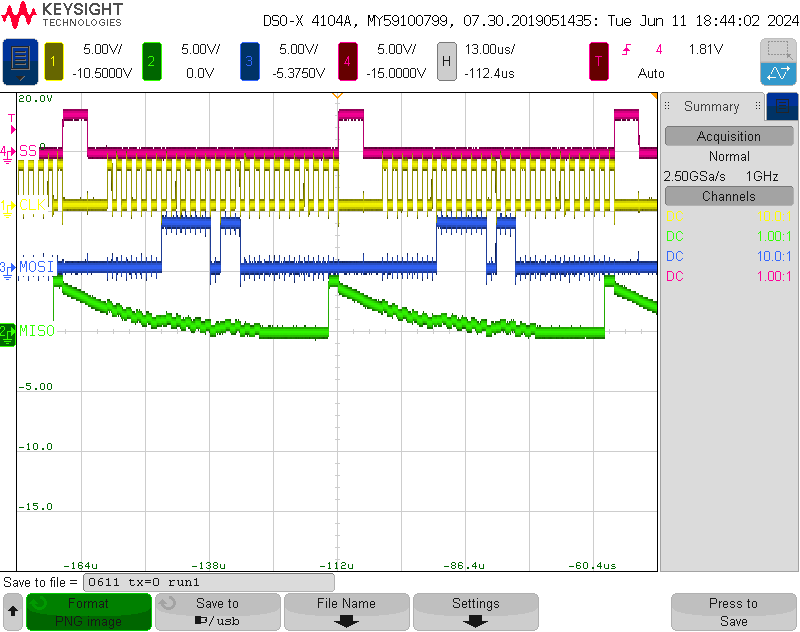
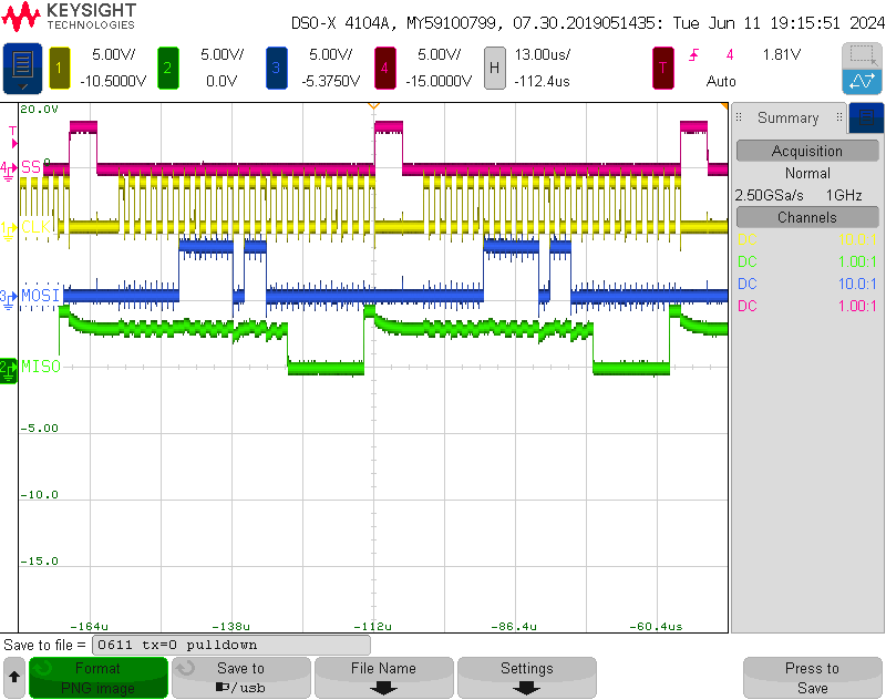
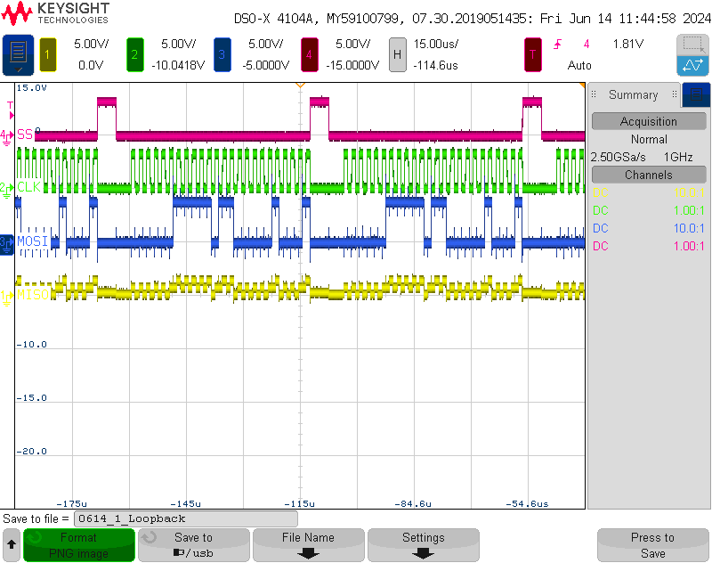
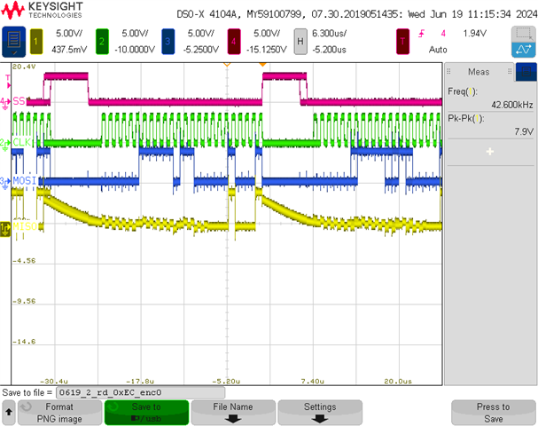
And I got this weird-looking MISO signal.

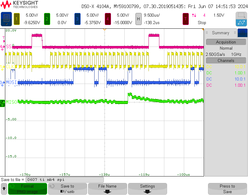
I first thought that the reason I got this signal was because I only have access to BIT 4 of the register however, writing 0x10 makes it access to other bits of the register as well.
So I also tried writing 0x11(=0b00010001) because I thought it might keep the BIT 0 value to '1'. However, the result was the same.
But I think it's not because the datasheet says that ' Register bits with constant ’0’ or ’1’ are ROM-based values and can not be changed through writing.' and I think writing 0x10 does not change the value of other registers that has values '0'.

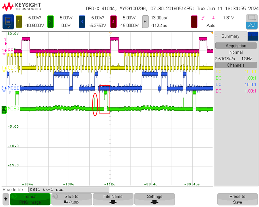
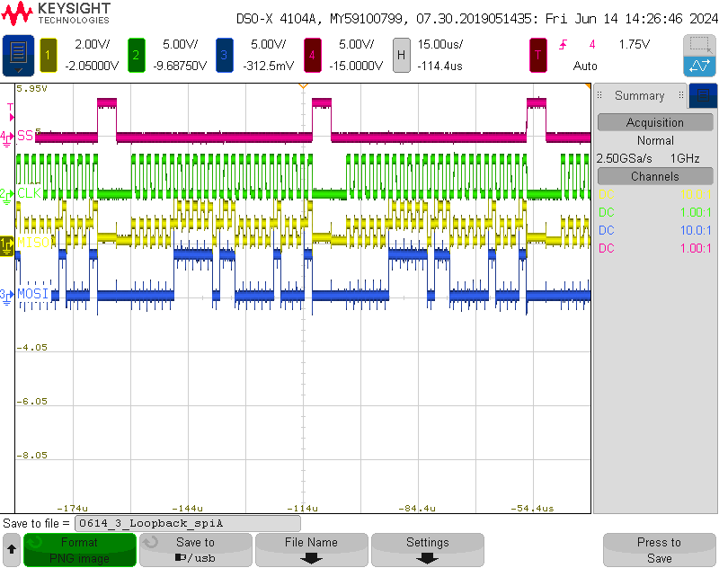
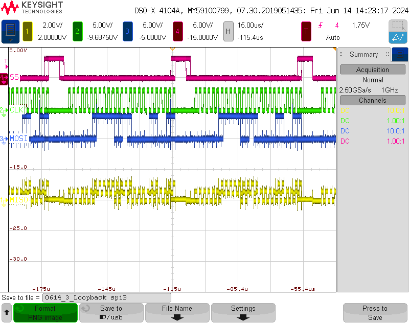
And I also tried setting MISO line to 'Push-pull output/pull-up enabled on INVERTED input' as I know this means 'Pull-down'.
But when I set the MISO to pull-down, I got a more weird signal.
The MISO suddenly worked as ACTIVE LOW.
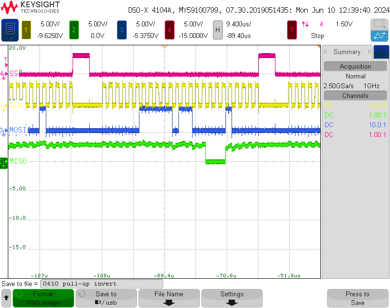
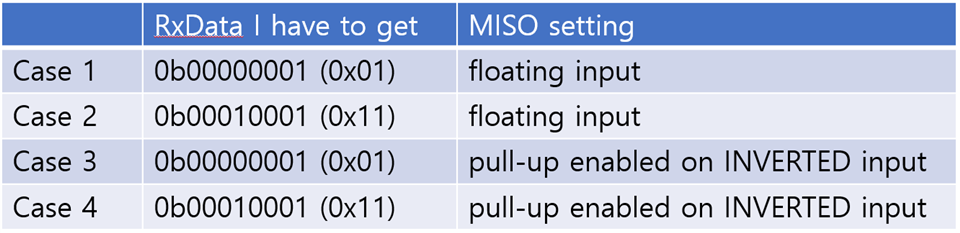
To sum up,
1. What's the problem with my SPI? Is it the code problem, or sysconfig setting problem? Or my misunderstanding of MB4 SPI protocol or settings?
2. Why does MISO work weirdly when I set it to 'Push-pull output/pull-up enabled on INVERTED input'?
3. Does 'Push-pull output/pull-up enabled on INVERTED input' mean Pull-down?
3. How can I solve this problem? 

  • Hi Sumin,

    Let me take a look and get back to you within 1-2 days.

    Best Regards,

    Aishwarya

  • Hi Aishwarya,
    Thanks for replying again:)

    After I wrote this question I had many different tries for the SPI and discovered something new.

    1. When I set TxData[2] = (uint16_t) (0U << 4); (== TxData[2] = 0;) / MISO 'Push-pull output/floating input'


    The data that has to be written is '0b00000001'.
    The value of the MISO data looks like 0b00000001.

    But the signal's shape goes weird at the end. I'm guessing there is some noise but I cannot guess 'where it is coming from' and 'why it happens'.


    2. When I set TxData[2] = (uint16_t) (1U << 4); (== TxData[2] = 0b00010000;) / MISO 'Push-pull output/floating input'

    The data that has to be written is '0b00010001'.
    But the MISO data's value doesn't look like it is getting 0b00010001. It seems like it is getting 0b00000010.
    I think BIT 4 (circle) looks like it has been triggered, but the signal is not strong enough for some reason. (I don't know if this is the right expression)  
    Also, the value '1' must be written in BIT 0 however, it's in BIT 1 (rectangle). I can't even guess why this happened. 

    And compared to case 1, the signal is clean and it seems there are no such noises.

    3. When I set TxData[2] = (uint16_t) (0U << 4); (== TxData[2] = 0;) / MISO 'Push-pull output/pull-up enabled on INVERTED input'

    4. When I set TxData[2] = (uint16_t) (1U << 4); (== TxData[2] = 0b00010000;) / MISO 'Push-pull output/pull-up enabled on INVERTED input'

    In cases 3 and 4, setting the MISO line to 'pull-up Invert' makes the signal to HIGH state.
    The value of the MISO data are the same as the cases 1 and 2 each.

    The SPI codes are the same as my first question and I only changed the values and the settings.
    I also organized the cases through the table for a better look.


    I'll be waiting for your reply then.
    Thanks again for your help:)

    Best regards,
    Sumin

  • Hi Sumin,

    3. Does 'Push-pull output/pull-up enabled on INVERTED input' mean Pull-down?

    The inverted refers to an inverted polarity on input. Is there a reason you need to qualify the GPIO as such? My recommendation is to leave it as the default and simply modify the SPI polarity and phase settings as needed. Since the second scope shot looks to be "cleaner", I would double check that the polarity and phase of the F2838x SPI and the MB4 SPI as well as other setup configurations matches. The transmission itself looks to be okay, I think.

    Best Regards,

    Aishwarya

  • Is there a reason you need to qualify the GPIO as such?

    I have an experience of using STM32 Nucleo board as an SPI master, and I had the similar problem as well. At that time setting 'pull-up' with CS pin and 'pull-down' with MISO pin solved the problem. So I thought that setting MISO as 'pull-down' will make the signal cleaner just like it worked with STM32.

    But I see that it doesn't work well with F28388D ...

  • Sumin,

    The chip select line is an active-low (idle-high) line by default, meaning communication to the peripheral device is allowed only when the chip select line is low. The MISO and MOSI lines are active-high (idle-low) by default. Noise is typically caused by the hardware setup, so I would check how you are grounding your scope probe (maybe try shorter probe), if there is any noise on the power supply, and see if you can isolate the issue as there is a chance some other protocol / part is causing it. Think about where the signal is coming from and where the signal is being probed. Note, there will be some noise due to SPI targe device internal switching.

    Best Regards,

    Aishwarya

  • Sumin, 

    Not sure why my post got deleted, but have you confirmed that the MB4 settings are correct? From our previous discussion, it seems that the F2838x SPI module is operating properly. The settings can be verified by putting the SPI in loopback mode.

    Best Regards,

    Aishwarya

  • Hi Aishwarya,

    I received an email from the TI E2E about the reply that you left about 6 hours ago.
    I don't know why I can't find it online but since I know the contents I will reply here.

    After I received your latest comments I checked my groundings and the circuit between MB4, F28388D, and the scope's probes.
    Each picture below is my circuit for the SPI and its probe, and the circuit schematic I drew.

    I configured the circuits based on informations written in the datasheets.
    The picture below is the pin configuration information of MB4 EVB.


    I've grounded all GND pins of MB4 and F28388D and all the probes to the same GND. As far as I see the groundings of this circuit look fine.

    Am I missing something in this?

    Best Regards,
    Sumin

  • Hi Aishwarya,

    As far as I know, the settings of the MB4 must be done by F28388D via SPI since it's working as SPI slave.
    SPI settings for MB4 have already been set and I think it cannot be changed because there is no information about the SPI settings of MB4 in the MB4 datasheet.

    The only thing I can change is selecting which interface to activate between 'PPI' and 'SPI'. (Left picture below)
    To activate SPI the CFGSPI must be set to 1, and in the EVB of MB4 by closing JP5 can set the CFGSPI=1. (Right picture below)
    I've checked my MB4 EVBoard and JP5 was in closed state.


    The settings can be verified by putting the SPI in loopback mode.

    I thought I was already in loopback mode.
    I understand that loopback mode is to write one data to the register in Slave device and reread the register's value to ensure that the data I sent is written well.
    Is the definition of loopback I know correct?
    What exactly does loopback mean if it's wrong?
    And how could I verify the settings if there is nothing I can set about the SPI settings of MB4?

    Best Regards,
    Sumin

  • Sumin,

    To clarify, I'm referring to internal loopback mode which can be done in SysConfig. Internal loopback refers to using one SPI module as both the peripheral and controller as opposed to using 2 SPI instances. By putting the SPI in internal loopback, you can verify data transmission, gpio configuration, and other software settings. Once SPI works in this mode, you can connect it back to the MB4. This would be the most straightforward approach to debugging SPI in this case. 

    Best Regards,

    Aishwarya

  • Hi Aishwarya,

    I tried the loopback as soon as I read your comment.
    And you were right. The loopback mode also got the MISO signal wrong.
    I got the signal like the picture below. There are no changes in the SPI code and the only change is setting the SPI in the loopback mode. 

    The picture on the right has the MISO signal 'scaled up' to 0-2V to 0-5V for a closer look at the signal.

    The weird thing about the MISO signal is,

    1. MISO acts the same as CLK. Since MISO is a data line the timing of the signal up/down should be the same as the MOSI however, you can see that it moves with the same timing with CLK from the picture on the right. 

    2. It looks like MISO has a bias. Before the first CLK starts, which means that before SPI starts, its reference of 'LOW STATE' is 0V. But when CLK starts, it acts the same as CLK, and the reference of 'LOW STATE' becomes Afternd after the SPI ends, the reference of 'LOW STATE' becomes 0V again.

    I have no idea why this happens...

    I also tried using a different SPI channel.
    So I changed the SPI channel to SPIB from SPIA.

    The result of MISO was the same.
    And the whole signal seems to be noise about the time axis. Its phase about the time keeps shaking.
    It seems that it has some jitter.

    I wonder,
    1. What is the reason for MISO acting like that?
    2. Why does using SPIB make a noisy signal about the time?

    Best Regards,
    Sumin

  • Sumin,

    Since the issue is present in loopback mode as well, you can rule out hardware connection issues. The clock schemes seem to be matching as well, but ensure you are setting a MCU SPI clock suitable for the given tSCLK (both), tM (F2838x), and tS (MB4). The values chosen on the controller side looks fine, but make sure the target is configured to this as well. This value should take into account the setup, hold, etc. times. Sometimes operating at too low/high of a clock speed can cause noise. There's also a high-speed mode bit you can use for SPI clocks that are up to 50 MHz for meeting timing requirements better.

    Best Regards,

    Aishwarya

  • Hi Aishwarya,

    I've thought about the loopback and I concluded that it's not odd to get such a pulse in MISO.
    Since I set the loopback mode by Sysconfig software, it was loopbacked 'internally' which means that the data will not 'go out' to the GPIO pin of MISO, so
    it was meaningless for me to probe to the GPIO MISO line.

    After I got my conclusion I checked if the rxData gets the txData value in the debug mode and I figured that they have the same values.
    I posted the code below.

    /*Included Files*/
    #include "driverlib.h"
    #include "device.h"
    #include "board.h"
    #include <stdio.h>


    //OP CODE
    #define WR_REG                      0x02
    #define RD_REG                      0x03
    #define RD_STS                      0x05
    #define WR_INS                      0x07
    
    //Register Addr
    #define SLAVELOC5                   0xEC
    
    
    /*private code*/
    #define nData                       3
    uint16_t TxData[nData] = {0,};
    uint16_t RxData[nData] = {0,};
    uint32_t txData = 0;
    uint32_t rxData = 0;
    uint16_t txDelay = 0;
    
    volatile uint16_t spirxemu_value = 0;
    volatile uint16_t spirxbuf_value = 0;
    
    
    uint32_t SPI_transmit24Bits_sumin(uint32_t base, uint32_t data, uint16_t txDelay);
    uint32_t SPI_pollingFIFOTransaction_sumin(uint32_t base, uint16_t charLength,
                               uint16_t *pTxBuffer, uint16_t *pRxBuffer,
                               uint16_t numOfWords, uint16_t txDelay);
    
    /*Main*/
    void main(void)
    {
        /*start settings*/
        // Initialize device clock and peripherals
        Device_init();
    
        // Disable pin locks and enable internal pullups.
        Device_initGPIO();
    
        // Initialize PIE and clear PIE registers. Disables CPU interrupts.
        Interrupt_initModule();
    
        // Initialize the PIE vector table with pointers to the shell Interrupt
        // Service Routines (ISR).
        Interrupt_initVectorTable();
    
        // Board initialization
        Board_init();
    
        // Enable Global Interrupt (INTM) and realtime interrupt (DBGM)
        EINT;
        ERTM;
    
    
        /*USER CODE*/
    
        TxData[0] = WR_REG;
        TxData[1] = SLAVELOC5;
    //    TxData[2] = (uint16_t) (1U << 4);
        TxData[2] = (uint16_t) (0x01 | (1U << 4));
        txData = ((uint32_t)TxData[0] << 16U) | ((uint32_t)TxData[1] << 8U) | (uint32_t)TxData[2];
        SPI_transmit24Bits(mySPIA_BASE, txData, txDelay);
    
        while(1)
        {
            TxData[0] = RD_REG;
            TxData[1] = SLAVELOC5;
            txData = ((uint32_t)TxData[0] << 16U) | ((uint32_t)TxData[1] << 8U) | (uint32_t)TxData[2];
            rxData = SPI_transmit24Bits_sumin(mySPIA_BASE, txData, txDelay);
    //        SPI_transmit24Bits(mySPIA_BASE, txData, txDelay);
    
            if(rxData != txData)
            {
                // Something went wrong. rData doesn't contain expected data.
                ESTOP0;
            }
        }
    }
    
    
    uint32_t
    SPI_transmit24Bits_sumin(uint32_t base, uint32_t data, uint16_t txDelay)
    {
        uint16_t i;
        uint16_t rxBuffer[3];
        uint16_t txBuffer[3];
    
        ASSERT(data < ((uint32_t)1U << 24U));
    
        //
        // Empty Receive buffer
        //
        for(i = 0U; i < 3U; i++)
        {
            rxBuffer[i] = 0U;
        }
    
        //
        // Fill Transmit buffer with appropriate data
        //
        txBuffer[0] = (uint16_t)(data >> 16U);   // data[23:16]
        txBuffer[1] = (uint16_t)(data) >> 8U;    // data[15:8]
        txBuffer[2] = (uint16_t)(data) & 0x00FFU; // data[7:0]
    
        //
        // Three 8-bits make a 24-bit
        // Character length = 8
        // number of bytes = 3
        //
        uint32_t rxdata = SPI_pollingFIFOTransaction_sumin(base, 8U, txBuffer, rxBuffer, 3U, txDelay);
        return rxdata;
    }


    uint32_t
    SPI_pollingFIFOTransaction_sumin(uint32_t base, uint16_t charLength,
                               uint16_t *pTxBuffer, uint16_t *pRxBuffer,
                               uint16_t numOfWords, uint16_t txDelay)
    {
        ASSERT(((HWREGH(base + SPI_O_CCR) & SPI_CCR_SPICHAR_M) + 1) == charLength);
    
        //
        // Reset the TX / RX FIFO buffers to default state
        //
        SPI_disableFIFO(base); // Disable FIFO register
        SPI_enableFIFO(base);  // Enable FIFO register
    
        //
        // Configure the FIFO Transmit Delay
        //
        SPI_setTxFifoTransmitDelay(base, txDelay);
    
        //
        // Determine the number of 16-level words from number of words to be
        // transmitted / received
        //
        uint16_t numOfSixteenWords = numOfWords / (uint16_t)SPI_FIFO_TXFULL;
    
        //
        // Determine the number of remaining words from number of words to be
        // transmitted / received
        //
        uint16_t remainingWords = numOfWords % (uint16_t)SPI_FIFO_TXFULL;
    
        uint16_t count = 0;
        uint16_t i = 0;
        uint16_t txBuffer_pos = 0;
        uint16_t rxBuffer_pos = 0;
    
        //
        // Number of transactions is based on numOfSixteenWords
        // Each transaction will transmit and receive 16 words.
        //
        while(count < numOfSixteenWords)
        {
            //
            // Fill-up the SPI Transmit FIFO buffers
            //
            for(i = 1; i <= (uint16_t)SPI_FIFO_TXFULL; i++)
            {
                SPI_writeDataBlockingFIFO(base, pTxBuffer[txBuffer_pos] <<
                                                (16U - charLength));
                txBuffer_pos++;
            }
    
            //
            // Wait till SPI Receive FIFO buffer is full
            //
            while(SPI_getRxFIFOStatus(base) < SPI_FIFO_RXFULL)
            {
            }
    
            //
            // Read the SPI Receive FIFO buffers
            //
            for(i = 1U; i <= (uint16_t)SPI_FIFO_RXFULL; i++)
            {
                if(pRxBuffer == NULL)
                {
                    SPI_readDataBlockingFIFO(base);
                }
                else
                {
                    pRxBuffer[rxBuffer_pos] = SPI_readDataBlockingFIFO(base);
                    rxBuffer_pos++;
                }
            }
    
            count++;
        }
    
        //
        // Number of transactions is based on remainingWords
        //
        for(i = 0U; i < remainingWords; i++)
        {
            SPI_writeDataBlockingFIFO(base, pTxBuffer[txBuffer_pos] <<
                                            (16U - charLength));
            txBuffer_pos++;
        }
    
        //
        // Wait till SPI Receive FIFO buffer remaining words
        //
        while((uint16_t)SPI_getRxFIFOStatus(base) < remainingWords)
        {
        }
    
        //
        // Read the SPI Receive FIFO buffers
        //
        for(i = 0; i < remainingWords; i++)
        {
            if(pRxBuffer == NULL)
            {
                SPI_readDataBlockingFIFO(base);
            }
            else
            {
                pRxBuffer[rxBuffer_pos] = SPI_readDataBlockingFIFO(base);
                rxBuffer_pos++;
            }
        }
    
        //
        // Disable SPI FIFO
        //
        SPI_disableFIFO(base);
    
    
        uint32_t data = 0;
        for(i = 0U; i < remainingWords; i++)
        {
            data |= ((uint32_t) pRxBuffer[i]) << 8*(remainingWords -1 - i);
        }
    
        return data;
    
    }
    
    //
    // End File
    //
    

    Is my conclusion about the loopback right?

    For the time setting, both MB4 and F2838x have a maximum SPI speed of 50MHz so the configuration between the master and slave are the same.
    I set the bit rate to 0.5MHz and I thought it was fast enough.
    But is it not fast enough to make such noise?

  • Sumin,

    Since I set the loopback mode by Sysconfig software, it was loopbacked 'internally' which means that the data will not 'go out' to the GPIO pin of MISO, so it was meaningless for me to probe to the GPIO MISO line.

    You can have a setup that brings the signals out to the pins using an "external" loopback if you wish to scope it.

    For the time setting, both MB4 and F2838x have a maximum SPI speed of 50MHz so the configuration between the master and slave are the same.
    I set the bit rate to 0.5MHz and I thought it was fast enough.
    But is it not fast enough to make such noise?

    Do you see the same noise also at 10 MHz and 20 MHz for example? 

    Also, on line 68, why do you have an additional transmit ? 

    Best Regards,

    Aishwarya

  • Hi Aishwarya,

    You can have a setup that brings the signals out to the pins using an "external" loopback if you wish to scope it.

    I also tried it after my recent reply and checked the value in debug mode since the signal will be the same.
    The Rx value got the same value as the Tx. 

    Do you see the same noise also at 10 MHz and 20 MHz for example? 

    When I rechecked the datasheet of the MB4, the maximum value of the CLK was normally 50Mhz but when reading the data the maximum value was 10MHz. So I tested it by changing it to 1MHz and it worked the same as when set to 0.5MHz.

    Also, on line 68, why do you have an additional transmit ? 

    This is for WRITING the value to the register 0xEC.
    What I wanted to do was WRITE the data, and then READ it back.


    I have a good news!
    I succeeded in transmitting and receiving the data properly!
    The wrong MISO data was because the encoder was not connected to the MB4 ... The hardware is always the problem ...
    I had no idea that such small points like this could cause the problem since my SPI was to access the register that has nothing to do with the encoder.

    I put the MISO data in the variable 'rxData' to see the data from MISO in debug mode.
    Since I wrote '1' in BIT 4 the desired rxData value is 0x11 and the oscilloscope signal and the rxData value both got the right data.

    But there is still an unsolved problem ...
    The signal still goes weird when one SPI transaction ends.
    However, the data value variable received is fine regardless of the weird signal.

    So I wonder,

    1. Why does the signal still look weird?
    2. Is it necessary to solve this signal problem?  

    Best regards,
    Sumin

  • Sumin,

    I agree, it is always good to triple check the hardware Slight smile  In terms of the signal, this is usually because of an incorrect data receival (software) or data format (configuration). You could check again to make sure the data is being transferred between the TX/RX buffers, SPIDAT, etc. The results might even just be the way the line is being scoped. Also, make sure you are using the latest C2000Ware 5.02 as the PollingNonFIFO function has been changed. (+) TMS320F280025C: Issues with manual control of CS pin in SPI when using driverlib functions

    Best Regards,

    Aishwarya