


Part Number: TMS320F2812
Tool/software:

Even though there are a few similar topics raised in the past, I couldn't address my issue.
I see the same issue on either bootloader or application build.
Changing page numbers causes memory issues and build errors.
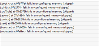
Here is our bootloader linker layout. The picture above also belongs to bootloader.
/*
// TI File $Revision: /main/2 $
// Checkin $Date: April 28, 2005   15:19:56 $
//###########################################################################
//
// FILE:	F2812.cmd
//
// TITLE:	Linker Command File For F2812 Device
//
//###########################################################################
// $TI Release: DSP281x Header Files V1.11 $
// $Release Date: September 26, 2007 $
//###########################################################################
*/

/* ======================================================
// For Code Composer Studio V2.2 and later
// ---------------------------------------
// In addition to this memory linker command file,
// add the header linker command file directly to the project.
// The header linker command file is required to link the
// peripheral structures to the proper locations within
// the memory map.
//
// The header linker files are found in <base>\DSP281x_Headers\cmd
//
// For BIOS applications add:      DSP281x_Headers_nonBIOS.cmd
// For nonBIOS applications add:   DSP281x_Headers_nonBIOS.cmd
========================================================= */

/* ======================================================
// For Code Composer Studio prior to V2.2
// --------------------------------------
// 1) Use one of the following -l statements to include the
// header linker command file in the project. The header linker
// file is required to link the peripheral structures to the proper
// locations within the memory map                                    */

/* Uncomment this line to include file only for non-BIOS applications */
/* -l DSP281x_Headers_nonBIOS.cmd */

/* Uncomment this line to include file only for BIOS applications */
/* -l DSP281x_Headers_BIOS.cmd */

/* 2) In your project add the path to <base>\DSP281x_headers\cmd to the
   library search path under project->build options, linker tab,
   library search path (-i).
/*========================================================= */

/* Define the memory block start/length for the F2812
   PAGE 0 will be used to organize program sections
   PAGE 1 will be used to organize data sections

   Notes:
         Memory blocks on F2812 are uniform (ie same
         physical memory) in both PAGE 0 and PAGE 1.
         That is the same memory region should not be
         defined for both PAGE 0 and PAGE 1.
         Doing so will result in corruption of program
         and/or data.
*/

MEMORY
{
PAGE 0:    /* Program Memory */
           /* Memory (RAM/FLASH/OTP) blocks can be moved to PAGE1 for data allocation */
/* DO NOT USE FLASH G,H,I,J.  Those are reserved for PROM Loader buffer*/
/* DO NOT USE FLASH B,C,D,E.  Those are reserved for Applications*/
/* DO NOT USE FLASH A.  Misprogramming A may lock up the flash*/
/* Use FLASH F for bootloader*/

   BOOT_START   : origin = 0x3D8000, length = 0x000002		/* branch to bootloader*/
   PFLASHIJ      : origin = 0x3D8002, length = 0x003FF6     /* Part of FLASHJ */
   BOOT_CRC	   : origin = 0x3DBFFF, length = 0x000001     /* Boot-loader's CRC*/
   BEGIN       : origin = 0x3F7FF6, length = 0x000002     /* Part of FLASHA.  Used for "boot to Flash" bootloader mode. */
   /* DO NOT TOUCH THE CSM area*/
   /* XINTF zone 7 available if MP/MCn=1 */
   ROM         : origin = 0x3FF000, length = 0x000FC0     /* Boot ROM available if MP/MCn=0 */
   RESET       : origin = 0x3FFFC0, length = 0x000002     /* part of boot ROM (MP/MCn=0) or XINTF zone 7 (MP/MCn=1) */
   VECTORS     : origin = 0x3FFFC2, length = 0x00003E     /* part of boot ROM (MP/MCn=0) or XINTF zone 7 (MP/MCn=1) */

PAGE 1 :   /* Data Memory */
           /* Memory (RAM/FLASH/OTP) blocks can be moved to PAGE0 for program allocation */
           /* Registers remain on PAGE1                                                  */

   RAMM0       : origin = 0x000000, length = 0x000400     /* on-chip RAM block M0 */
   RAMM1       : origin = 0x000400, length = 0x000400     /* on-chip RAM block M1 */
   RAML0       : origin = 0x008000, length = 0x001000     /* on-chip RAM block L0 */
   RAML1       : origin = 0x009000, length = 0x001000     /* on-chip RAM block L1, holds downloaded PROM Loader */

   /* 8 words at the end of FLASHF are reserved for file system (Boot CRC, Base, Length)*/

   /*   RAMH0   reserved to download PROM loader */
   /* declare external RAM */

   EXT_DSRAM   : origin = 0xA0000, length = 0x20000   /* For programm downloading */
   EXT_PSRAM   : origin = 0x80000, length = 0x10000   /* for bootlader still 52K free */
   EXT_PROMLOADER: origin = 0x90000, length = 0x10000   /* reserved section for promloader*/

   /* Standard DSP281x non-BIOS memory mapping*/
   DEV_EMU     : origin = 0x000880, length = 0x000180     /* device emulation registers */
   PIE_VECT    : origin = 0x000D00, length = 0x000100     /* PIE Vector Table */
   FLASH_REGS  : origin = 0x000A80, length = 0x000060     /* FLASH registers */
   CSM         : origin = 0x000AE0, length = 0x000010     /* code security module registers */
   XINTF       : origin = 0x000B20, length = 0x000020     /* external interface registers */
   CPU_TIMER0  : origin = 0x000C00, length = 0x000008     /* CPU Timer0 registers (CPU Timer1 and Timer2 are reserved for BIOS)*/
   CPU_TIMER1  : origin = 0x000C08, length = 0x000008     /* CPU Timer1 registers */
   PIE_CTRL    : origin = 0x000CE0, length = 0x000020     /* PIE control registers */
   ECANA       : origin = 0x006000, length = 0x000040     /* eCAN control and status registers */
   ECANA_LAM   : origin = 0x006040, length = 0x000040     /* eCAN local acceptance masks */
   ECANA_MOTS  : origin = 0x006080, length = 0x000040     /* eCAN message object time stamps */
   ECANA_MOTO  : origin = 0x0060C0, length = 0x000040     /* eCAN object time-out registers */
   ECANA_MBOX  : origin = 0x006100, length = 0x000100     /* eCAN mailboxes */
   SYSTEM      : origin = 0x007010, length = 0x000020     /* System control registers */
   SPIA        : origin = 0x007040, length = 0x000010     /* SPI registers */
   SCIA        : origin = 0x007050, length = 0x000010     /* SCI-A registers */
   XINTRUPT    : origin = 0x007070, length = 0x000010     /* external interrupt registers */
   GPIOMUX     : origin = 0x0070C0, length = 0x000020     /* GPIO mux registers */
   GPIODAT     : origin = 0x0070E0, length = 0x000020     /* GPIO data registers */
   ADC         : origin = 0x007100, length = 0x000020     /* ADC registers */
   EVA         : origin = 0x007400, length = 0x000040     /* Event Manager A registers */
   EVB         : origin = 0x007500, length = 0x000040     /* Event Manager B registers */
   SCIB        : origin = 0x007750, length = 0x000010     /* SCI-B registers */
   MCBSPA      : origin = 0x007800, length = 0x000040     /* McBSP registers */
   CSM_PWL     : origin = 0x3F7FF8, length = 0x000008     /* Part of FLASHA.  CSM password locations. */
}

/* Allocate sections to memory blocks.
   Note:
         codestart user defined section in DSP28_CodeStartBranch.asm used to redirect code
                   execution when booting to flash
         ramfuncs  user defined section to store functions that will be copied from Flash into RAM
*/

SECTIONS
{
   /* Allocate program areas: */
   .cinit              : > PFLASHIJ      PAGE = 0
   .pinit              : > PFLASHIJ,     PAGE = 0
   .text               : > PFLASHIJ      PAGE = 0
   codestart           : > BEGIN       PAGE = 0
   bootstart		   : > BOOT_START  PAGE = 0


   /* Allocate uninitalized data sections: */
   .stack              : > RAMM0       PAGE = 1
   .ebss               : > RAML1       PAGE = 1
   .esysmem            : > RAML0       PAGE = 1

   /* Initalized sections go in Flash */
   /* For SDFlash to program these, they must be allocated to page 0 */
   .econst             : > PFLASHIJ      PAGE = 0
   .switch             : > PFLASHIJ      PAGE = 0

   /*crcTables*/
   .crcTable		   : > PFLASHIJ		PAGE = 0
   /*allocate prom loader memory location*/
   .boot_loader		   : > EXT_PSRAM	PAGE = 1
   /*Data RAM*/
   section_ext_sram	 : > EXT_DSRAM,      PAGE = 1

   /*after determining the CRC, replace this and redownload through JTAG */
   .boot_crc        : > BOOT_CRC     PAGE = 0
   /*Don't need IQmath*/


   /* .reset is a standard section used by the compiler.  It contains the */
   /* the address of the start of _c_int00 for C Code.   /*
   /* When using the boot ROM this section and the CPU vector */
   /* table is not needed.  Thus the default type is set here to  */
   /* DSECT  */
   .reset              : > RESET,      PAGE = 0, TYPE = DSECT
   vectors             : > VECTORS     PAGE = 0, TYPE = DSECT
   /* Standard DSP281x non-BIOS memory mapping*/
   PieVectTableFile : > PIE_VECT,   PAGE = 1

/*** Peripheral Frame 0 Register Structures ***/
   DevEmuRegsFile    : > DEV_EMU,     PAGE = 1
   FlashRegsFile     : > FLASH_REGS,  PAGE = 1
   CsmRegsFile       : > CSM,         PAGE = 1
   XintfRegsFile     : > XINTF,       PAGE = 1
   CpuTimer0RegsFile : > CPU_TIMER0,  PAGE = 1
   CpuTimer1RegsFile : > CPU_TIMER1,  PAGE = 1
   PieCtrlRegsFile   : > PIE_CTRL,    PAGE = 1

/*** Peripheral Frame 1 Register Structures ***/
   ECanaRegsFile     : > ECANA,       PAGE = 1
   ECanaLAMRegsFile  : > ECANA_LAM    PAGE = 1
   ECanaMboxesFile   : > ECANA_MBOX   PAGE = 1
   ECanaMOTSRegsFile : > ECANA_MOTS   PAGE = 1
   ECanaMOTORegsFile : > ECANA_MOTO   PAGE = 1

/*** Peripheral Frame 2 Register Structures ***/
   SysCtrlRegsFile   : > SYSTEM,      PAGE = 1
   SpiaRegsFile      : > SPIA,        PAGE = 1
   SciaRegsFile      : > SCIA,        PAGE = 1
   XIntruptRegsFile  : > XINTRUPT,    PAGE = 1
   GpioMuxRegsFile   : > GPIOMUX,     PAGE = 1
   GpioDataRegsFile  : > GPIODAT      PAGE = 1
   AdcRegsFile       : > ADC,         PAGE = 1
   EvaRegsFile       : > EVA,         PAGE = 1
   EvbRegsFile       : > EVB,         PAGE = 1
   ScibRegsFile      : > SCIB,        PAGE = 1
   McbspaRegsFile    : > MCBSPA,      PAGE = 1

/*** Code Security Module Register Structures ***/
   CsmPwlFile        : > CSM_PWL,     PAGE = 1

}


