Part Number: TMS320F28377S
Tool/software:
Hi team,
We have a few questions concerning power up of the part following up on the related thread.
In the designs, VDD is 1.2V. VDDOSC/VDDIO/VDD3V3FL are tied to 3.3V.
One of the designs delays the start of the VDD ramp (1.2V) for a millisecond after VDDOSC/VDDIO/VDD3V3FL and has a high ramp rate to start.
Otherwise, VDD and VDDOSC/VDDIO/VDD3V3FL are always powered on/off together.
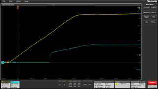
Please see the images below.
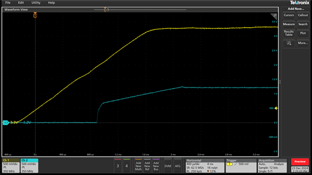
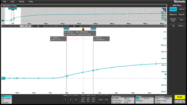
In this case:
VDDOSC is powered when VDD is off for a period of 1 ms at power up.
The initial ramp rate of VDD is 26k v/s for the first 10 us before settling at under 2000 v/s.
Does this meet the requirements:
"VDDOSC and VDD must be powered on and off at the same time. VDDOSC should not be powered on when VDD is off.”
Supply Ramp Rate between 330 and 10^5 V/s.
Thanks for the support,
Luke