This thread has been locked.

If you have a related question, please click the "Ask a related question" button in the top right corner. The newly created question will be automatically linked to this question.

TMS320F28379D: TMS320F28379D : SCI boot 1

Part Number: TMS320F28379D
Other Parts Discussed in Thread: UNIFLASH, C2000WARE

Tool/software:

Hi,

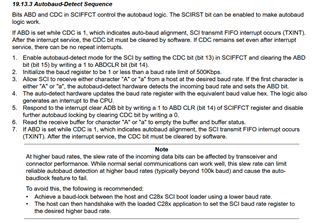
We have a requirement to flash the application using serial communication. To achieve this, we enabled SCI Boot Mode 1 since we are using SCI-A with GPIO pins 28 and 29.

Here are the steps we followed to enable SCI Boot Mode 1 and load the application:

  1. Set the OTP register Z1-BOOTCTRL (0x7801E) = 0x4955815A.
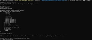
  2. Use the Serial Flash Programmer utility provided by TI.
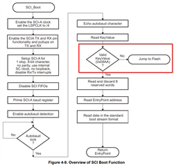
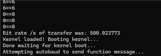
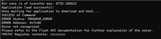
  3. The kernel and application were successfully flashed onto the board, and the system ran correctly. However, after a power cycle, the CPU goes into Hibernate Boot mode (refer to RTM: Figure 4-6, CPU1 Standalone and Hibernate Boot Flow).

Please help us configure the system to boot from flash so that the application runs correctly after the power cycle.

Regards,
Aditya

  • Hi Aditya,

    Unfortunately, the BOOTCTRL register is limited in this case. Given that GET mode only allows one custom boot option to be programmed (0x81 here), the only way to get the device to boot to flash after reset is if the autobaud key value is not valid (!= 0x08AA). 

    More recent devices (F280013x, F28003x, F2838x, F28P55x, etc.) have the BOOTDEF register to address this by supporting up to 8 boot options to be selected, and would make this a non-issue. 

    Best,

    Matt

  • Hi Matt,

    Thanks so much!

    If we change the autobaud key value as mentioned, will we still be able to upgrade the firmware using SCI boot 1 afterward?

    Regards,

    Aditya

  • Hi Aditya,

    Yes, as long as the the KeyValue is valid (0x08AA) you'll be able to use SCI boot 1 to upgrade firmware. Otherwise, the device will boot to flash. You'll have to find a way to fail the KeyValue check so the boot ROM boots to flash instead. 

    Best,

    Matt

  • I will assume that this issue is resolved and close the thread, as its been several weeks without a response. Please open a new thread if that's not the case.

  • Hi Matt,

    Issue stil not resloved

    Please find the below details:

    Problem statement : Use SCI Boot mode 1 for firmware upgrade, after that firmware start in every power cycle.

    Perform Action :

    1. Set the OTP register Z1-BOOTCTRL (0x7801E) = 0x4955815A, using uniflash.
    2. DSP goes into boot mode.
    3. Used the Serial Flash Programmer utility provided by TI.
    4. Application upgraded using bootloader and lauch perfectly from FLASH.
    5. Both Bootmode pin (Gpio 72 and 84) set high (GET mode).
    6. After power cycle DSP does not start the application (FLASH application). and also we are not sending any data on SCI A port(same which is use for firmeare upgrade)
    7. We also flash the application using JTAG into flash area, but still after power cycle application does not start.

    As you mentioned in earlier message that if the bootloader receive invalid autobuad key value then it will start the flash application.

    So in our case, after power cycle we are not sending any data on SCI port, that means it is not reciving any autobaud key value and it should start the application, which is not happening.

    Please let us know if we are missing any step's or need to do any changes in existing steps

    Regards,

    Aditya

  • Hi Aditya,

    Uint16 SCIA_GetWordData()
    {
       Uint16 wordData;
       Uint16 byteData;
    
       wordData = 0x0000;
       byteData = 0x0000;
    
       // Fetch the LSB and verify back to the host
       while(SciaRegs.SCIRXST.bit.RXRDY != 1) { }
       wordData =  (Uint16)SciaRegs.SCIRXBUF.bit.RXDT;
       SciaRegs.SCITXBUF = wordData;
    
       // Fetch the MSB and verify back to the host
       while(SciaRegs.SCIRXST.bit.RXRDY != 1) { }
       byteData =  (Uint16)SciaRegs.SCIRXBUF.bit.RXDT;
       SciaRegs.SCITXBUF = byteData;
    
       // form the wordData from the MSB:LSB
       wordData |= (byteData << 8);
    
       return wordData;
    }

    we are not sending any data on SCI port, that means it is not reciving any autobaud key value and it should start the application, which is not happening.

    This is a function from the SCI ROM bootloader (C2000Ware_X_XX_XX_XX\libraries\boot_rom\f2837xd\revB\rom_sources\F2837x_bootROM\cpu01-bootROM\source), if you're not sending any data to the SCI port, then the device will continue to wait until something is received. An incorrect autobaud key needs to be sent at this point.

    Best,

    Matt

  • Dear Matt,

    since our system get installed at remote location, so It is not possible to send an incorrect autobaud key at every power cycle.

    is there any other way to modify rom bootloader. so no need to send an incorrect autobaud key.

    we have another quirey releated to boot mode selection pins ( gpio 72 and 84),for flash booting, which mode we should select using boot mode pin.

    Regards,

    Aditya

  • Hi Aditya,

    No, unfortunately it is not possible to modify the boot ROM. The only way you'll be able to achieve SCI booting with GPIO28/29 and flash boot mode on F2837xD devices is if you make your own custom SCI bootloader in the flash. Note that it would be possible to use the ROM bootloaders if you used GPIO84/85 for SCI.

    You can do this by modifying the SCI flash kernels (C2000Ware_X_XX_XX_XX\device_support\f2837xd\examples\dual\F2837xD_sci_flash_kernels) to be built and execute in the flash. The application (which is loaded into another flash bank) can then receive a command for a firmware upgrade and jump to the SCI bootloader when necessary.

    we have another quirey releated to boot mode selection pins ( gpio 72 and 84),for flash booting, which mode we should select using boot mode pin.

    You'll want to configure GPIO72 and GPIO84 both to 1 to enable "Get/Flash" boot mode. Get boot mode, by default on an unprogrammed device (ie. the BOOTCTRL register in the OTP is not programmed) boots to Flash.

    Best,

    Matt

  • Dear Matt,

    I hope you're doing well.

    We have modified the SCI flash kernels (C2000Ware_X_XX_XX_XX\device_support\f2837xd\examples\dual\F2837xD_sci_flash_kernels) to support an alternate SCI boot mode using GPIO 28 and 29. However, we are encountering the following issues:

    1. While debugging, I am receiving the error:
      "Texas Instruments XDS100v2 USB Debug Probe_0/C28xx_CPU1 : Target must be connected before loading program."
      The debugger is connected, and the connection test shows success, but the error still occurs.

    2. Despite flashing the code, when trying the firmware update using the TI utility, we run the following command:

      .\serial_flash_programmer.exe -d f2837xD -k .\F2837xD_sci_flash_kernels_cpu01.txt -a .\blinky_dc_cpu01.txt -b 9600 -p COM7 -v

      The process gets stuck at the "attempting autobuad" step.

    Additionally, do we need to use the F2837xD_sci_flash_kernels_cpu01.txt kernel each time during the firmware upgrade?

    Could you kindly guide us on how to properly perform a firmware upgrade using a custom SCI bootloader?

    Thank you in advance for your support.

    Best regards,
    Aditya

  • Hi Aditya,

    "Texas Instruments XDS100v2 USB Debug Probe_0/C28xx_CPU1 : Target must be connected before loading program."

    This thread may be helpful: https://e2e.ti.com/support/tools/code-composer-studio-group/ccs/f/code-composer-studio-forum/781790/ccs-lp-cc2652rb-automatic-loading-of-program-not-possible-if-2-different-launch-pads-are-connected-to-same-pc/2890700#2890700

    As for your custom bootloader, there's a few things I want to clarify:

    1. Is the SCI flash kernel built for the RAM or Flash?
      1. If the kernel is built for the RAM (which it is by default in C200Ware), then you're loading the kernel in with the ROM bootloader using a different set of GPIO assignments than the alternate GPIO assignment you intend to use. Therefore, the serial flash programmer won't be able to detect the autobaud once the kernel takes over execution.
      2. If the SCI kernel is built for the Flash, you can load the kernel into the Flash (using CCS or UniFlash). Then, you have to branch to the custom bootloader (from the application or by booting to the bootloader's flash entry point) and use serial_flash_programmer_appIn.exe to load the application code through the custom bootloader into the Flash. 

    In your case, you're going to need to build the custom bootloader for Flash execution and follow the flow in option (b).

    Best,

    Matt

  • Hi Matt,

    We build the SCI kernel for the flash, we successfuly debug it but when we use serial flash programmer.exe provide by TI, it get error and stop the execution.

    Below error msg we get 

    What things we do wroung please suggest the correct approch.

    Regards, 

    Aditya

  • Hi Aditya,

    Usually this happens because the baud-rate is too high or some noise is interfering with communication.

    1. What serial interface are you using for communication with the device?
    2. What is your device setup (is this a custom board, LaunchPad, controlCard, etc.)?
    3. How are you invoking the serial_flash_programmer_appIn.exe?

    Best,

    Matt

  • Hi Matt,

    I’m using a USB-to-serial(RS232) adapter for communication with the device. The setup is based on a custom board we’re working on, so it’s not a LaunchPad or controlCard.

    We are invoking the serial flash programmer using below command,

    " .\serial_flash_programmer.exe -d f2837xD -k .\F2837xD_sci_flash_kernels_cpu01.txt -a .\blinky_dc_cpu01.txt -b 9600 -p COM14 -v"

    Regards,

    Aditya

  • Hi Aditya,

    Are you attempting to load the SCI kernel built for flash using the ROM bootloader? The bootloaders in the ROM can only load code into the RAM.

    If so, you need to program kernel into the flash first (using CCS, UniFlash, third-party tool, etc.) and then use the serial_flash_programmer_appIn.exe to only download the application (after booting the device to the kernel in flash). You can invoke the application only executable without the "-k" argument:

    .\serial_flash_programmer_appIn.exe -d f2837xD -a .\blinky_dc_cpu01.txt -b 9600 -p COM14 -v

    Best,

    Matt

  • Hi Matt,

    I follow the same step as you mentioned,

    1. Build the Kernel for Flash.

    2. Load the kernel using CCS.

    3. Use Serial_flash_programmer_appln.exe 

    Command :   .\serial_flash_programmer_appln.exe -d f2837xD -a .\blinky_dc_cpu01.txt -b 9600 -p COM14 -v

    But we get NACK error. please find the below details,

    Regards,

    Aditya

  • Hi Aditya,

    Are the application's flash sections 128-bit aligned? In the linker command file's SECTIONS, add a comma and "ALIGN(8)" after each line where a section is allocated to flash.

    Best,

    Matt

  • Hi Matt,

    We do as you suggest, add "ALIGN(8)" after each line where section is allocated to flash.

    but get the same result ara as above.

    Regards,

    Aditya

  • Hi Matt,

    We successfully loaded the application, but we’re encountering a program error afterward.

    Here are the details:

    After running command "RUN CPU1" or performing a power cycle, neither the custom bootloader nor the application boots.

    Could you please advise how we can start the application after a power cycle?

    Best regards,

    Aditya

  • Hi Aditya,

    The kernel is reporting a programming error, can you check the FMSTAT register in CCS to view the reported failure status? Can you also share your application linker command file (.cmd)?

    For more details, please see the FMSTAT register field description in the F2837xD Flash API reference guide:

    Best,

    Matt

  • Hi Matt,

    please find the application command file

    /*
    //###########################################################################
    // FILE: flash_programming_cpu1_FLASH.cmd
    // TITLE: Linker Command File For all F28X7x devices
    //###########################################################################
    // $TI Release: F2837xD Support Library v200 $
    // $Release Date: Tue Jun 21 13:00:02 CDT 2016 $
    // $Copyright: Copyright (C) 2013-2016 Texas Instruments Incorporated -
    // http://www.ti.com/ ALL RIGHTS RESERVED $
    //###########################################################################
    */

    /* ======================================================
    // For Code Composer Studio V2.2 and later
    // ---------------------------------------
    // In addition to this memory linker command file,
    // add the header linker command file directly to the project.
    // The header linker command file is required to link the
    // peripheral structures to the proper locations within
    // the memory map.
    // The header linker files are found in <base>\F2837xD_headers\cmd
    // For BIOS applications add: F28X7x_Headers_BIOS.cmd
    // For nonBIOS applications add: F28X7x_Headers_nonBIOS.cmd
    ========================================================= */

    /* Define the memory block start/length for the F28X7x
    PAGE 0 will be used to organize program sections
    PAGE 1 will be used to organize data sections

    Notes:
    Memory blocks on F28M3Xx are uniform (ie same
    physical memory) in both PAGE 0 and PAGE 1.
    That is the same memory region should not be
    defined for both PAGE 0 and PAGE 1.
    Doing so will result in corruption of program
    and/or data.

    Contiguous SARAM memory blocks or flash sectors can be
    be combined if required to create a larger memory block.
    */

    MEMORY
    {
    PAGE 0: /* Program Memory */
    /* Memory (RAM/FLASH) blocks can be moved to PAGE1 for data allocation */
    /* BEGIN is used for the "boot to Flash" bootloader mode */

    BEGIN : origin = 0x080000, length = 0x000002
    RAMM0 : origin = 0x000122, length = 0x0002DE
    RAMD0 : origin = 0x00B000, length = 0x000800
    RAMLS03 : origin = 0x008000, length = 0x002000
    /* RAMLS1 : origin = 0x008800, length = 0x000800
    RAMLS2 : origin = 0x009000, length = 0x000800
    RAMLS3 : origin = 0x009800, length = 0x000800 */
    RAMLS4 : origin = 0x00A000, length = 0x000800
    RAMGS14 : origin = 0x01A000, length = 0x001000
    RAMGS15 : origin = 0x01B000, length = 0x001000
    RESET : origin = 0x3FFFC0, length = 0x000002

    /* Flash sectors */
    FLASHA : origin = 0x080002, length = 0x001FFE /* on-chip Flash */
    FLASHB : origin = 0x082000, length = 0x002000 /* on-chip Flash */
    FLASHC : origin = 0x084000, length = 0x002000 /* on-chip Flash */
    FLASHD : origin = 0x086000, length = 0x00A000 /* on-chip Flash */
    FLASHE : origin = 0x090000, length = 0x002000 /* on-chip Flash */
    FLASHF : origin = 0x092000, length = 0x006000 /* on-chip Flash */
    FLASHG : origin = 0x098000, length = 0x008000 /* on-chip Flash */
    FLASHH : origin = 0x0A0000, length = 0x008000 /* on-chip Flash */
    FLASHI : origin = 0x0A8000, length = 0x008000 /* on-chip Flash */
    FLASHJ : origin = 0x0B0000, length = 0x008000 /* on-chip Flash */
    FLASHK : origin = 0x0B8000, length = 0x002000 /* on-chip Flash */
    FLASHL : origin = 0x0BA000, length = 0x002000 /* on-chip Flash */
    FLASHM : origin = 0x0BC000, length = 0x002000 /* on-chip Flash */
    FLASHN : origin = 0x0BE000, length = 0x002000 /* on-chip Flash */

    PAGE 1 : /* Data Memory */
    /* Memory (RAM/FLASH) blocks can be moved to PAGE0 for program allocation */

    BOOT_RSVD : origin = 0x000002, length = 0x000120 /* Part of M0, BOOT rom will use this for stack */
    RAMM1 : origin = 0x000400, length = 0x000400 /* on-chip RAM block M1 */
    RAMD1 : origin = 0x00B800, length = 0x000800

    RAMLS5 : origin = 0x00A800, length = 0x000800

    RAMGS0 : origin = 0x00C000, length = 0x00B000
    /*RAMGS1 : origin = 0x00D000, length = 0x001000*/
    /*RAMGS2 : origin = 0x00E000, length = 0x001000*/
    /*RAMGS3 : origin = 0x00F000, length = 0x001000
    RAMGS4 : origin = 0x010000, length = 0x001000
    RAMGS5 : origin = 0x011000, length = 0x001000
    RAMGS6 : origin = 0x012000, length = 0x001000
    RAMGS7 : origin = 0x013000, length = 0x001000
    RAMGS8 : origin = 0x014000, length = 0x001000
    RAMGS9 : origin = 0x015000, length = 0x001000
    RAMGS10 : origin = 0x016000, length = 0x001000*/
    RAMGS11 : origin = 0x017000, length = 0x001000
    RAMGS12 : origin = 0x018000, length = 0x001000
    RAMGS13 : origin = 0x019000, length = 0x001000


    CPU2TOCPU1RAM : origin = 0x03F800, length = 0x000400
    CPU1TOCPU2RAM : origin = 0x03FC00, length = 0x000400
    }


    SECTIONS
    {

    /* Allocate program areas: */
    .cinit : > FLASHD PAGE = 0, ALIGN(8)
    .pinit : > FLASHD, PAGE = 0, ALIGN(8)
    .text : >> FLASHD | FLASHE |FLASHH | FLASHI PAGE = 0, ALIGN(8)
    codestart : > BEGIN PAGE = 0, ALIGN(8)

    GROUP
    {
    ramfuncs
    dclfuncs
    { -l F021_API_F2837xD_FPU32.lib}

    } LOAD = FLASHD,
    RUN = RAMLS03,
    LOAD_START(_RamfuncsLoadStart),
    LOAD_SIZE(_RamfuncsLoadSize),
    LOAD_END(_RamfuncsLoadEnd),
    RUN_START(_RamfuncsRunStart),
    RUN_SIZE(_RamfuncsRunSize),
    RUN_END(_RamfuncsRunEnd),
    PAGE = 0, ALIGN(8)

    /* Allocate uninitalized data sections: */
    .stack : > RAMM1 PAGE = 1
    .ebss : >> RAMLS5 | RAMGS0 PAGE = 1
    .esysmem : > RAMLS5 PAGE = 1

    /* Initalized sections go in Flash */
    .econst : >> FLASHF | FLASHG PAGE = 0, ALIGN(8)
    .switch : > FLASHD PAGE = 0, ALIGN(8)

    .reset : > RESET, PAGE = 0, TYPE = DSECT /* not used, */

    Filter_RegsFile : > RAMGS0, PAGE = 1

    SHARERAMGS0 : > RAMGS0, PAGE = 1
    SHARERAMGS1 : > RAMGS11, PAGE = 1

    /* Flash Programming Buffer */
    BufferDataSection : > RAMD1, PAGE = 1, ALIGN(4)

    /* The following section definitions are required when using the IPC API Drivers */
    GROUP : > CPU1TOCPU2RAM, PAGE = 1
    {
    PUTBUFFER
    PUTWRITEIDX
    GETREADIDX
    }

    GROUP : > CPU2TOCPU1RAM, PAGE = 1
    {
    GETBUFFER : TYPE = DSECT
    GETWRITEIDX : TYPE = DSECT
    PUTREADIDX : TYPE = DSECT
    }

    }

    /*
    //===========================================================================
    // End of file.
    //===========================================================================
    */

    Regards,

    Aditya

  • Hi Aditya,

    The kernel is reporting a programming error, can you check the FMSTAT register in CCS to view the reported failure status?

    Can you check the FMSTAT register in CCS after the kernel attempts to load the application?

    Can you also share your SCI flash kernel's linker command file?

    Best,

    Matt

  • Hi Matt,

    I made some changes to the command linker file of the application, and after that, I was able to flash the application using the custom bootloader. It runs properly as expected.

    However, after a power cycle, the custom bootloader is invoked but does not jump to the application, how we jump to the application ?

    We add some timeout in bootloader but it not work properly.

    Could you please check the attached command linker files for both the bootloader and the application?

    Bootloader Command file.

    MEMORY
    {
    PAGE 0 :  /* Program Memory */
              /* Memory (RAM/FLASH) blocks can be moved to PAGE1 for data allocation */
       RAMM0           	: origin = 0x000122, length = 0x0002DE
       RAMD0           	: origin = 0x00B000, length = 0x000800
       RAMLS0          	: origin = 0x008000, length = 0x000800
       RAMLS1          	: origin = 0x008800, length = 0x000800
       RAMLS2      		: origin = 0x009000, length = 0x000800
       RAMLS3      		: origin = 0x009800, length = 0x000800
       RAMLS4      		: origin = 0x00A000, length = 0x000800
       RAMGS14          : origin = 0x01A000, length = 0x001000
       RAMGS15          : origin = 0x01B000, length = 0x001000
       RESET           	: origin = 0x3FFFC0, length = 0x000002
       
    
    #ifdef __TI_COMPILER_VERSION__
       #if __TI_COMPILER_VERSION__ >= 20012000
    GROUP {      /* GROUP memory ranges for crc/checksum of entire flash */
       #endif
    #endif
    
       /* BEGIN is used for the "boot to Flash" bootloader mode   */
       BEGIN           	: origin = 0x080000, length = 0x000002
    
       /* Flash sectors */
       FLASHA           : origin = 0x080002, length = 0x001FFE	/* on-chip Flash */
       FLASHB           : origin = 0x082000, length = 0x002000	/* on-chip Flash */
       FLASHC           : origin = 0x084000, length = 0x002000	/* on-chip Flash */
       FLASHD           : origin = 0x086000, length = 0x002000	/* on-chip Flash */
       FLASHE           : origin = 0x088000, length = 0x008000	/* on-chip Flash */
       FLASHF           : origin = 0x090000, length = 0x008000	/* on-chip Flash */
       FLASHG           : origin = 0x098000, length = 0x008000	/* on-chip Flash */
       FLASHH           : origin = 0x0A0000, length = 0x008000	/* on-chip Flash */
       FLASHI           : origin = 0x0A8000, length = 0x008000	/* on-chip Flash */
       FLASHJ           : origin = 0x0B0000, length = 0x008000	/* on-chip Flash */
       FLASHK           : origin = 0x0B8000, length = 0x002000	/* on-chip Flash */
       FLASHL           : origin = 0x0BA000, length = 0x002000	/* on-chip Flash */
       FLASHM           : origin = 0x0BC000, length = 0x002000	/* on-chip Flash */
       FLASHN           : origin = 0x0BE000, length = 0x002000	/* on-chip Flash */   
    #ifdef __TI_COMPILER_VERSION__
      #if __TI_COMPILER_VERSION__ >= 20012000
    }  crc(_table_name, algorithm=C28_CHECKSUM_16)
      #endif
    #endif
    
    PAGE 1 : /* Data Memory */
             /* Memory (RAM/FLASH) blocks can be moved to PAGE0 for program allocation */
    
       BOOT_RSVD       : origin = 0x000002, length = 0x000120     /* Part of M0, BOOT rom will use this for stack */
       RAMM1           : origin = 0x000400, length = 0x000400     /* on-chip RAM block M1 */
       RAMD1           : origin = 0x00B800, length = 0x000800
    
       RAMLS5      : origin = 0x00A800, length = 0x000800
    
       RAMGS0      : origin = 0x00C000, length = 0x001000
       RAMGS1      : origin = 0x00D000, length = 0x001000
       RAMGS2      : origin = 0x00E000, length = 0x001000
       RAMGS3      : origin = 0x00F000, length = 0x001000
       RAMGS4      : origin = 0x010000, length = 0x001000
       RAMGS5      : origin = 0x011000, length = 0x001000
       RAMGS6      : origin = 0x012000, length = 0x001000
       RAMGS7      : origin = 0x013000, length = 0x001000
       RAMGS8      : origin = 0x014000, length = 0x001000
       RAMGS9      : origin = 0x015000, length = 0x001000
       RAMGS10     : origin = 0x016000, length = 0x001000
       RAMGS11     : origin = 0x017000, length = 0x001000
       RAMGS12     : origin = 0x018000, length = 0x001000
       RAMGS13     : origin = 0x019000, length = 0x001000
    
       
       CPU2TOCPU1RAM   : origin = 0x03F800, length = 0x000400
       CPU1TOCPU2RAM   : origin = 0x03FC00, length = 0x000400
    }
    
    
    SECTIONS
    {
       /* Allocate program areas: */
       .cinit              : > FLASHB      PAGE = 0, ALIGN(8)
       .pinit              : > FLASHB,     PAGE = 0, ALIGN(8)
       .text               : >> FLASHB | FLASHC | FLASHD | FLASHE      PAGE = 0, ALIGN(8)
       codestart           : > BEGIN       PAGE = 0, ALIGN(8)
    
    #ifdef __TI_COMPILER_VERSION__
       #if __TI_COMPILER_VERSION__ >= 15009000
        .TI.ramfunc : {} LOAD = FLASHD,
                             RUN = RAMLS0 | RAMLS1 | RAMLS2 |RAMLS3,
                             LOAD_START(_RamfuncsLoadStart),
                             LOAD_SIZE(_RamfuncsLoadSize),
                             LOAD_END(_RamfuncsLoadEnd),
                             RUN_START(_RamfuncsRunStart),
                             RUN_SIZE(_RamfuncsRunSize),
                             RUN_END(_RamfuncsRunEnd),
                             PAGE = 0, ALIGN(8)
       #else
       ramfuncs            : LOAD = FLASHD,
                             RUN = RAMLS0 | RAMLS1 | RAMLS2 |RAMLS3,
                             LOAD_START(_RamfuncsLoadStart),
                             LOAD_SIZE(_RamfuncsLoadSize),
                             LOAD_END(_RamfuncsLoadEnd),
                             RUN_START(_RamfuncsRunStart),
                             RUN_SIZE(_RamfuncsRunSize),
                             RUN_END(_RamfuncsRunEnd),
                             PAGE = 0, ALIGN(8)
       #endif
    #endif
    						 
       /* Allocate uninitalized data sections: */
       .stack              : > RAMM1        PAGE = 1
       .ebss               : >> RAMLS5 | RAMGS0 | RAMGS1       PAGE = 1
       .esysmem            : > RAMLS5       PAGE = 1
    
       /* Initalized sections go in Flash */
       .econst             : >> FLASHF | FLASHG | FLASHH      PAGE = 0, ALIGN(8)
       .switch             : > FLASHB      PAGE = 0, ALIGN(8)
       
       .reset              : > RESET,     PAGE = 0, TYPE = DSECT /* not used, */
    
       Filter_RegsFile     : > RAMGS0,	   PAGE = 1
       
       SHARERAMGS0		: > RAMGS0,		PAGE = 1
       SHARERAMGS1		: > RAMGS1,		PAGE = 1
       
       /* The following section definitions are required when using the IPC API Drivers */ 
        GROUP : > CPU1TOCPU2RAM, PAGE = 1 
        {
            PUTBUFFER 
            PUTWRITEIDX 
            GETREADIDX 
        }
        
        GROUP : > CPU2TOCPU1RAM, PAGE = 1
        {
            GETBUFFER :    TYPE = DSECT
            GETWRITEIDX :  TYPE = DSECT
            PUTREADIDX :   TYPE = DSECT
        }  
    
       /* crc/checksum section configured as COPY section to avoid including in executable */
       .TI.memcrc          : type = COPY
        
    }
    
    /*
    //===========================================================================
    // End of file.
    //===========================================================================
    */
    

    Application Command file

    /*
    //###########################################################################
    // FILE:    flash_programming_cpu1_FLASH.cmd
    // TITLE:   Linker Command File For all F28X7x devices
    //###########################################################################
    // $TI Release: F2837xD Support Library v200 $
    // $Release Date: Tue Jun 21 13:00:02 CDT 2016 $
    // $Copyright: Copyright (C) 2013-2016 Texas Instruments Incorporated -
    //             http://www.ti.com/ ALL RIGHTS RESERVED $
    //###########################################################################
    */
    
    /* ======================================================
    // For Code Composer Studio V2.2 and later
    // ---------------------------------------
    // In addition to this memory linker command file,
    // add the header linker command file directly to the project.
    // The header linker command file is required to link the
    // peripheral structures to the proper locations within
    // the memory map.
    // The header linker files are found in <base>\F2837xD_headers\cmd
    // For BIOS applications add:      F28X7x_Headers_BIOS.cmd
    // For nonBIOS applications add:   F28X7x_Headers_nonBIOS.cmd
    ========================================================= */
    
    /* Define the memory block start/length for the F28X7x
       PAGE 0 will be used to organize program sections
       PAGE 1 will be used to organize data sections
    
       Notes:
             Memory blocks on F28M3Xx are uniform (ie same
             physical memory) in both PAGE 0 and PAGE 1.
             That is the same memory region should not be
             defined for both PAGE 0 and PAGE 1.
             Doing so will result in corruption of program
             and/or data.
    
             Contiguous SARAM memory blocks or flash sectors can be
             be combined if required to create a larger memory block.
    */
    
    MEMORY
    {
    PAGE 0:    /* Program Memory */
              /* Memory (RAM/FLASH) blocks can be moved to PAGE1 for data allocation */
              /* BEGIN is used for the "boot to Flash" bootloader mode   */
    
      BEGIN           	: origin = 0x098000, length = 0x000002
       RAMM0           	: origin = 0x000122, length = 0x0002DE
       RAMD0           	: origin = 0x00B000, length = 0x000800
       RAMLS03          : origin = 0x008000, length = 0x002000
    /*	RAMLS1           : origin = 0x008800, length = 0x000800
        RAMLS2           : origin = 0x009000, length = 0x000800
        RAMLS3           : origin = 0x009800, length = 0x000800 */
       RAMLS4      		: origin = 0x00A000, length = 0x000800
       RAMGS14          : origin = 0x01A000, length = 0x001000
       RAMGS15          : origin = 0x01B000, length = 0x001000
       RESET           	: origin = 0x3FFFC0, length = 0x000002
    
    	/* Flash sectors */
       FLASHA           : origin = 0x080002, length = 0x001FFE	/* on-chip Flash */
       FLASHB           : origin = 0x082000, length = 0x002000	/* on-chip Flash */
       FLASHC           : origin = 0x084000, length = 0x002000	/* on-chip Flash */
       FLASHD           : origin = 0x086000, length = 0x002000	/* on-chip Flash */
       FLASHE           : origin = 0x090000, length = 0x002000	/* on-chip Flash */
       FLASHF           : origin = 0x092000, length = 0x006000	/* on-chip Flash */
       FLASHG           : origin = 0x098002, length = 0x007FFE	/* on-chip Flash */
       FLASHH           : origin = 0x0A0000, length = 0x008000	/* on-chip Flash */
       FLASHI           : origin = 0x0A8000, length = 0x008000	/* on-chip Flash */
       FLASHJ           : origin = 0x0B0000, length = 0x008000	/* on-chip Flash */
       FLASHK           : origin = 0x0B8000, length = 0x002000	/* on-chip Flash */
       FLASHL           : origin = 0x0BA000, length = 0x002000	/* on-chip Flash */
       FLASHM           : origin = 0x0BC000, length = 0x002000	/* on-chip Flash */
       FLASHN           : origin = 0x0BE000, length = 0x002000	/* on-chip Flash */
    
    PAGE 1 :   /* Data Memory */
             /* Memory (RAM/FLASH) blocks can be moved to PAGE0 for program allocation */
    
        BOOT_RSVD       : origin = 0x000002, length = 0x000120     /* Part of M0, BOOT rom will use this for stack */
    	RAMM1           : origin = 0x000400, length = 0x000400     /* on-chip RAM block M1 */
        RAMD1           : origin = 0x00B800, length = 0x000800
    
        RAMLS5      : origin = 0x00A800, length = 0x000800
    
    	RAMGS0          : origin = 0x00C000, length = 0x00B000
    	/*RAMGS1          : origin = 0x00D000, length = 0x001000*/
    	/*RAMGS2          : origin = 0x00E000, length = 0x001000*/
    	/*RAMGS3          : origin = 0x00F000, length = 0x001000
    	RAMGS4          : origin = 0x010000, length = 0x001000
    	RAMGS5          : origin = 0x011000, length = 0x001000
    	RAMGS6          : origin = 0x012000, length = 0x001000
    	RAMGS7          : origin = 0x013000, length = 0x001000
    	RAMGS8          : origin = 0x014000, length = 0x001000
    	RAMGS9          : origin = 0x015000, length = 0x001000
    	RAMGS10         : origin = 0x016000, length = 0x001000*/
    	RAMGS11         : origin = 0x017000, length = 0x001000
    	RAMGS12         : origin = 0x018000, length = 0x001000
    	RAMGS13         : origin = 0x019000, length = 0x001000
    
    
       CPU2TOCPU1RAM   : origin = 0x03F800, length = 0x000400
       CPU1TOCPU2RAM   : origin = 0x03FC00, length = 0x000400
    }
    
    
    SECTIONS
    {
    
       /* Allocate program areas: */
       .cinit              : > FLASHG      PAGE = 0, ALIGN(8)
       .pinit              : > FLASHG,     PAGE = 0, ALIGN(8)
       .text               : >> FLASHG | FLASHH |FLASHI | FLASHJ | FLASHK     PAGE = 0, ALIGN(8)
       codestart           : > BEGIN	PAGE = 0, ALIGN(8)
       
        GROUP
        {
            ramfuncs
            dclfuncs
            { -l F021_API_F2837xD_FPU32.lib}
         
        } LOAD = FLASHG,
          RUN  = RAMLS03, 
          LOAD_START(_RamfuncsLoadStart),
          LOAD_SIZE(_RamfuncsLoadSize),
          LOAD_END(_RamfuncsLoadEnd),
          RUN_START(_RamfuncsRunStart),
          RUN_SIZE(_RamfuncsRunSize),
          RUN_END(_RamfuncsRunEnd),
          PAGE = 0, ALIGN(8)
    
       /* Allocate uninitalized data sections: */
       .stack              : > RAMM1       PAGE = 1
       .ebss               : >> RAMLS5 | RAMGS0       PAGE = 1
       .esysmem            : > RAMLS5       PAGE = 1
    
       /* Initalized sections go in Flash */
       .econst             : >> FLASHF | FLASHG       PAGE = 0, ALIGN(8)
       .switch             : > FLASHG      PAGE = 0, ALIGN(8)
    
       .reset              : > RESET,     PAGE = 0, TYPE = DSECT /* not used, */
    
       Filter_RegsFile     : > RAMGS0,	   PAGE = 1
    
       SHARERAMGS0		: > RAMGS0,		PAGE = 1
       SHARERAMGS1		: > RAMGS11,		PAGE = 1
    
       /* Flash Programming Buffer */
       BufferDataSection : > RAMD1, PAGE = 1, ALIGN(4)   
       
       /* The following section definitions are required when using the IPC API Drivers */ 
        GROUP : > CPU1TOCPU2RAM, PAGE = 1 
        {
            PUTBUFFER 
            PUTWRITEIDX 
            GETREADIDX 
        }
    
        GROUP : > CPU2TOCPU1RAM, PAGE = 1
        {
            GETBUFFER :    TYPE = DSECT
            GETWRITEIDX :  TYPE = DSECT
            PUTREADIDX :   TYPE = DSECT
        }  
    
    }
    
    /*
    //===========================================================================
    // End of file.
    //===========================================================================
    */


    Regards,

    Aditya

  • Hi Aditya,

    Please verify there's no overlaps/conflicts between the application and bootloader in the flash. Currently, the .econst sections overlap (in FLASHF, FLASHG, and FLASHH) which will be problematic when flash programming.

    Aside: when attempting to do a LIVE firmware update (i.e. going back to the bootloader from the application without reset), greater care will also have to be taken with the RAM.

    We add some timeout in bootloader but it not work properly.

    Can you share the code you're implementing for the timeout?

    Best,

    Matt

  • Hi Matt,

    The timeout in the bootloader works as expected, and after 5 seconds, the application runs.

    However, my serial peripherals, SCI A and SCI B, are not working when the application flash using bootloader. When we flash only the application, the serial peripherals work properly.

    Could you please check and advise?

    Check the below code for timeout.

    void SCIA_AutobaudLock(void)
    {
        Uint16 byteData;
        Uint32 nWait = 0;
        //
        // Must prime baud register with >= 1
        //
        SciaRegs.SCILBAUD.bit.BAUD = 1;
    
        //
        // Prepare for autobaud detection
        // Set the CDC bit to enable autobaud detection
        // and clear the ABD bit
        //
        SciaRegs.SCIFFCT.bit.CDC = 1;
        SciaRegs.SCIFFCT.bit.ABDCLR = 1;
    
        //
        // Wait until we correctly read an
        // 'A' or 'a' and lock
        //
        while(SciaRegs.SCIFFCT.bit.ABD != 1 && nWait <= 5000) {
            nWait++;
            DELAY_US(1000);
        }
        if(nWait > 5000){
            bSetGotoFlash = 1;
        }
        else{
            //
            // After autobaud lock, clear the ABD and CDC bits
            //
            SciaRegs.SCIFFCT.bit.ABDCLR = 1;
            SciaRegs.SCIFFCT.bit.CDC = 0;
    
            while(SciaRegs.SCIRXST.bit.RXRDY != 1) { }
            byteData = SciaRegs.SCIRXBUF.bit.SAR;
            SciaRegs.SCITXBUF.bit.TXDT = byteData;
        }
        return;
    }

    and return to application address.

        SCIA_AutobaudLock();
    
        if(bSetGotoFlash)
        {
            EALLOW;
            WdRegs.SCSR.all = 0;    //enable WDRST
            WdRegs.WDCR.all = 0x28; //enable WD
            EDIS;
    
            EntryAddr = 0xaff96;
            return(EntryAddr);
        }

    Regards, 

    Aditya.

  • Hi Aditya,

    Your timeout code violates the autobaud-detect sequence, as described in the TRM. You need to disable further autobaud locking by clearing the CDC bit in a timeout event as well.

    void SCIA_AutobaudLock(void)
    {
        Uint16 byteData;
        Uint32 nWait = 0;
        //
        // Must prime baud register with >= 1
        //
        SciaRegs.SCILBAUD.bit.BAUD = 1;
    
        //
        // Prepare for autobaud detection
        // Set the CDC bit to enable autobaud detection
        // and clear the ABD bit
        //
        SciaRegs.SCIFFCT.bit.CDC = 1;
        SciaRegs.SCIFFCT.bit.ABDCLR = 1;
    
        //
        // Wait until we correctly read an
        // 'A' or 'a' and lock
        //
        while(SciaRegs.SCIFFCT.bit.ABD != 1 && nWait <= 5000) {
            nWait++;
            DELAY_US(1000);
        }
        if(nWait > 5000){
            bSetGotoFlash = 1;
            
            SciaRegs.SCIFFCT.bit.ABDCLR = 1;
            SciaRegs.SCIFFCT.bit.CDC = 0;
        }
        else{
            //
            // After autobaud lock, clear the ABD and CDC bits
            //
            SciaRegs.SCIFFCT.bit.ABDCLR = 1;
            SciaRegs.SCIFFCT.bit.CDC = 0;
    
            while(SciaRegs.SCIRXST.bit.RXRDY != 1) { }
            byteData = SciaRegs.SCIRXBUF.bit.SAR;
            SciaRegs.SCITXBUF.bit.TXDT = byteData;
        }
        return;
    }

    Best,

    Matt

  • Hi Matt,

    We tried clearing the CDC bit, but encountered some issues.

    Is there a way to perform a clean boot-up from the bootloader before jumping to the application?

    Regards,
    Aditya

  • Hi Aditya,

    Are you performing a LB to the application codestart? From the linker command file for the application you provided, this is at 0x098000. Why are you branching to 0x0AFF96?

    Best,

    Matt

  • Hi Matt,

    we referred to the map file and saw that the entry symbol _c_int00 was located at 0x0AFF96, which led us to branch to that address from the bootloader.

    We did try branching to 0x098000 as well, but noticed that the SCI module still doesn't get invoked

    Regards,
    Aditya

  • Hi Aditya,

    I see. In general, you'll want to branch to the codestartbranch.asm for the application code. What codestartbranch.asm are you using for the bootloader?

    And to confirm: you've removed all the overlaps in the flash between kernel and application?

    Best,

    Matt

  • Hi Matt,

    Yes, we have removed all overlaps. There are no flash overlaps between the kernel and the application.

    Please find the below .asm file we use.

    ;// TI File $Revision: /main/2 $
    ;// Checkin $Date: December 7, 2011   18:25:05 $
    ;//###########################################################################
    ;//
    ;// FILE:  F2837xD_CodeStartBranch._asm	
    ;//
    ;// TITLE: Branch for redirecting code execution after boot. 
    ;//
    ;// For these examples, code_start is the first code that is executed after
    ;// exiting the boot ROM code. 
    ;//
    ;// The codestart section in the linker cmd file is used to physically place
    ;// this code at the correct memory location.  This section should be placed 
    ;// at the location the BOOT ROM will re-direct the code to.  For example, 
    ;// for boot to FLASH this code will be located at 0x3f7ff6. 
    ;//
    ;// In addition, the example F2837xD projects are setup such that the codegen
    ;// entry point is also set to the code_start label.  This is done by linker 
    ;// option -e in the project build options.  When the debugger loads the code,
    ;// it will automatically set the PC to the "entry point" address indicated by
    ;// the -e linker option.  In this case the debugger is simply assigning the PC, 
    ;// it is not the same as a full reset of the device. 
    ;// 
    ;// The compiler may warn that the entry point for the project is other then
    ;//  _c_init00.  _c_init00 is the C environment setup and is run before 
    ;// main() is entered. The code_start code will re-direct the execution 
    ;// to _c_init00 and thus there is no worry and this warning can be ignored. 
    ;// 
    ;//###########################################################################
    ;// $TI Release: F2837xD Support Library v3.04.00.00 $
    ;// $Release Date: Sun Mar 25 13:26:04 CDT 2018 $
    ;// $Copyright:
    ;// Copyright (C) 2013-2018 Texas Instruments Incorporated - http://www.ti.com/
    ;//
    ;// Redistribution and use in source and binary forms, with or without 
    ;// modification, are permitted provided that the following conditions 
    ;// are met:
    ;// 
    ;//   Redistributions of source code must retain the above copyright 
    ;//   notice, this list of conditions and the following disclaimer.
    ;// 
    ;//   Redistributions in binary form must reproduce the above copyright
    ;//   notice, this list of conditions and the following disclaimer in the 
    ;//   documentation and/or other materials provided with the   
    ;//   distribution.
    ;// 
    ;//   Neither the name of Texas Instruments Incorporated nor the names of
    ;//   its contributors may be used to endorse or promote products derived
    ;//   from this software without specific prior written permission.
    ;// 
    ;// THIS SOFTWARE IS PROVIDED BY THE COPYRIGHT HOLDERS AND CONTRIBUTORS 
    ;// "AS IS" AND ANY EXPRESS OR IMPLIED WARRANTIES, INCLUDING, BUT NOT 
    ;// LIMITED TO, THE IMPLIED WARRANTIES OF MERCHANTABILITY AND FITNESS FOR
    ;// A PARTICULAR PURPOSE ARE DISCLAIMED. IN NO EVENT SHALL THE COPYRIGHT 
    ;// OWNER OR CONTRIBUTORS BE LIABLE FOR ANY DIRECT, INDIRECT, INCIDENTAL, 
    ;// SPECIAL, EXEMPLARY, OR CONSEQUENTIAL DAMAGES (INCLUDING, BUT NOT 
    ;// LIMITED TO, PROCUREMENT OF SUBSTITUTE GOODS OR SERVICES; LOSS OF USE,
    ;// DATA, OR PROFITS; OR BUSINESS INTERRUPTION) HOWEVER CAUSED AND ON ANY
    ;// THEORY OF LIABILITY, WHETHER IN CONTRACT, STRICT LIABILITY, OR TORT 
    ;// (INCLUDING NEGLIGENCE OR OTHERWISE) ARISING IN ANY WAY OUT OF THE USE 
    ;// OF THIS SOFTWARE, EVEN IF ADVISED OF THE POSSIBILITY OF SUCH DAMAGE.
    ;// $
    ;//###########################################################################
    
    ***********************************************************************
    
    WD_DISABLE	.set	1		;set to 1 to disable WD, else set to 0
    
        .global code_start
        .global _ExitBoot
    	.ref _main
    
    ***********************************************************************
    * Function: codestart section
    *
    * Description: Branch to code starting point
    ***********************************************************************
    
        .sect "codestart"
    
    code_start:
            LB wd_disable       ;Branch to watchdog disable code
    
    ;end codestart section
    
    ***********************************************************************
    * Function: wd_disable
    *
    * Description: Disables the watchdog timer
    ***********************************************************************
        .if WD_DISABLE == 1
    
        .text
    __stack:    .usect ".stack",0
    
    wd_disable:
        SETC OBJMODE        ;Set OBJMODE for 28x object code
        EALLOW              ;Enable EALLOW protected register access
        MOVZ DP, #7029h>>6  ;Set data page for WDCR register
        MOV @7029h, #0068h  ;Set WDDIS bit in WDCR to disable WD
        EDIS                ;Disable EALLOW protected register access
    ;    LB _c_int00         ;Branch to start of boot._asm in RTS library
    	LCR _main
    ; Cleanup and exit.  At this point the EntryAddr
    ; is located in the ACC register
        BF  _ExitBoot,UNC
        .endif
    
    ;end wd_disable
    
    
    ;-----------------------------------------------
    ; _ExitBoot
    ;-----------------------------------------------
    ;-----------------------------------------------
    ;This module cleans up after the boot loader
    ;
    ; 1) Make sure the stack is deallocated.
    ;    SP = 0x400 after exiting the boot
    ;    loader
    ; 2) Push 0 onto the stack so RPC will be
    ;    0 after using LRETR to jump to the
    ;    entry point
    ; 2) Load RPC with the entry point
    ; 3) Clear all XARn registers
    ; 4) Clear ACC, P and XT registers
    ; 5) LRETR - this will also clear the RPC
    ;    register since 0 was on the stack
    ;-----------------------------------------------
    
    _ExitBoot:
    
    ;-----------------------------------------------
    ;   Insure that the stack is deallocated
    ;-----------------------------------------------
    
        MOV SP,#__stack
    
    ;-----------------------------------------------
    ; Clear the bottom of the stack.  This will endup
    ; in RPC when we are finished
    ;-----------------------------------------------
    
        MOV  *SP++,#0
        MOV  *SP++,#0
    
    ;-----------------------------------------------
    ; Load RPC with the entry point as determined
    ; by the boot mode.  This address will be returned
    ; in the ACC register.
    ;-----------------------------------------------
    
        PUSH ACC
        POP  RPC
    
    ;-----------------------------------------------
    ; Put registers back in their reset state.
    ;
    ; Clear all the XARn, ACC, XT, and P and DP
    ; registers
    ;
    ; NOTE: Leave the device in C28x operating mode
    ;       (OBJMODE = 1, AMODE = 0)
    ;-----------------------------------------------
        ZAPA
        MOVL  XT,ACC
        MOVZ  AR0,AL
        MOVZ  AR1,AL
        MOVZ  AR2,AL
        MOVZ  AR3,AL
        MOVZ  AR4,AL
        MOVZ  AR5,AL
        MOVZ  AR6,AL
        MOVZ  AR7,AL
        MOVW  DP, #0
    
    ;------------------------------------------------
    ;   Restore ST0 and ST1.  Note OBJMODE is
    ;   the only bit not restored to its reset state.
    ;   OBJMODE is left set for C28x object operating
    ;   mode.
    ;
    ;  ST0 = 0x0000     ST1 = 0x0A0B
    ;  15:10 OVC = 0    15:13      ARP = 0
    ;   9: 7  PM = 0       12       XF = 0
    ;      6   V = 0       11  M0M1MAP = 1
    ;      5   N = 0       10  reserved
    ;      4   Z = 0        9  OBJMODE = 1
    ;      3   C = 0        8    AMODE = 0
    ;      2  TC = 0        7 IDLESTAT = 0
    ;      1 OVM = 0        6   EALLOW = 0
    ;      0 SXM = 0        5     LOOP = 0
    ;                       4      SPA = 0
    ;                       3     VMAP = 1
    ;                       2    PAGE0 = 0
    ;                       1     DBGM = 1
    ;                       0     INTM = 1
    ;-----------------------------------------------
    
        MOV  *SP++,#0
        MOV  *SP++,#0x0A0B
        POP  ST1
        POP  ST0
    
    ;------------------------------------------------
    ;   Jump to the EntryAddr as defined by the
    ;   boot mode selected and continue execution
    ;-----------------------------------------------
    
        LRETR
    
    ;eof ----------
    
    	.end
    	
    ;//===========================================================================
    ;// End of file.
    ;//===========================================================================
    

    My issue get reslove after reset "ClkCfgRegs".

    But i did not know why in exit routin in .asm file, this register not get reset.

    Regards,

    Aditya.

  • Hi Aditya,

    I don't believe ClkCfgRegs is intended to be reset in the exit boot routine.

    Did you initialize SysCtrl (i.e. initialize the peripheral clocks) in your application when it didn't work before?

    Best,

    Matt

  • Hi Matt,

    Yes we have initialize sysctrl which is already call in "F2837xD_sci_flash_kernels_cpu01.c" 

    // Step 1. Initialize System Control:
    // Enable Peripheral Clocks
    // This example function is found in the F2837xD_SysCtrl.c file.
    //
        InitSysCtrl(); //PLL activates

    Is there any issue in my "CodeStartBranch._asm" ? which i have already share with you.

    Regards,

    Aditya

  • Hi Aditya,

    The CodeStartBranch file looks good.

    Do you initialize SysCtrl again in your application too? It is possible one of the SCI dependencies is still getting re-initialized/modified when jumping to the starting address of the application. For example, if the clocks get re-initialized.

    Best,

    Matt

  • Hi,

    Since this thread hasn't been replied to in a month, I will assume it is resolved and close the thread.

    Best,

    Matt

  • Hi Matt,

    Right now we get the we are facing below issue while upgrade the new version of firmware, but while upgrade the pervious version it get upgrade succesfully without any error. but now we get this type of error or some time it get stuck at 46 00 86 FE 06 00.

    Please check below Uploaded files, 

    firmware.txt -  get the above error while upgrading the firmware.

    400000000384.v5.1.txt - working txt file of pervious firmware version.

    400000000384.v5.1.txtfirmware.txt

    This my cmd file use for create both firmware version

    /*
    //###########################################################################
    // FILE:    flash_programming_cpu1_FLASH.cmd
    // TITLE:   Linker Command File For all F28X7x devices
    //###########################################################################
    // $TI Release: F2837xD Support Library v200 $
    // $Release Date: Tue Jun 21 13:00:02 CDT 2016 $
    // $Copyright: Copyright (C) 2013-2016 Texas Instruments Incorporated -
    //             http://www.ti.com/ ALL RIGHTS RESERVED $
    //###########################################################################
    */
    
    /* ======================================================
    // For Code Composer Studio V2.2 and later
    // ---------------------------------------
    // In addition to this memory linker command file,
    // add the header linker command file directly to the project.
    // The header linker command file is required to link the
    // peripheral structures to the proper locations within
    // the memory map.
    // The header linker files are found in <base>\F2837xD_headers\cmd
    // For BIOS applications add:      F28X7x_Headers_BIOS.cmd
    // For nonBIOS applications add:   F28X7x_Headers_nonBIOS.cmd
    ========================================================= */
    
    /* Define the memory block start/length for the F28X7x
       PAGE 0 will be used to organize program sections
       PAGE 1 will be used to organize data sections
    
       Notes:
             Memory blocks on F28M3Xx are uniform (ie same
             physical memory) in both PAGE 0 and PAGE 1.
             That is the same memory region should not be
             defined for both PAGE 0 and PAGE 1.
             Doing so will result in corruption of program
             and/or data.
    
             Contiguous SARAM memory blocks or flash sectors can be
             be combined if required to create a larger memory block.
    */
    
    MEMORY
    {
    PAGE 0:    /* Program Memory */
              /* Memory (RAM/FLASH) blocks can be moved to PAGE1 for data allocation */
              /* BEGIN is used for the "boot to Flash" bootloader mode   */
    
      BEGIN           	: origin = 0x086000, length = 0x000002
       RAMM0           	: origin = 0x000122, length = 0x0002DE
       RAMD0           	: origin = 0x00B000, length = 0x000800
       RAMLS03          : origin = 0x008000, length = 0x002000
    /*	RAMLS1           : origin = 0x008800, length = 0x000800
        RAMLS2           : origin = 0x009000, length = 0x000800
        RAMLS3           : origin = 0x009800, length = 0x000800 */
       RAMLS4      		: origin = 0x00A000, length = 0x000800
       RAMGS14          : origin = 0x01A000, length = 0x001000
       RAMGS15          : origin = 0x01B000, length = 0x001000
       RESET           	: origin = 0x3FFFC0, length = 0x000002
    
    	/* Flash sectors */
       FLASHA           : origin = 0x080000, length = 0x002000	/* on-chip Flash */
       FLASHB           : origin = 0x082000, length = 0x002000	/* on-chip Flash */
       FLASHC           : origin = 0x084000, length = 0x002000	/* on-chip Flash */
       FLASHD           : origin = 0x086002, length = 0x001FFE	/* on-chip Flash */
       FLASHE           : origin = 0x088000, length = 0x008000	/* on-chip Flash */
       FLASHF           : origin = 0x090000, length = 0x008000	/* on-chip Flash */
       FLASHG           : origin = 0x098000, length = 0x008000	/* on-chip Flash */
       FLASHH           : origin = 0x0A0000, length = 0x008000	/* on-chip Flash */
       FLASHI           : origin = 0x0A8000, length = 0x008000	/* on-chip Flash */
       FLASHJ           : origin = 0x0B0000, length = 0x008000	/* on-chip Flash */
       FLASHK           : origin = 0x0B8000, length = 0x002000	/* on-chip Flash */
       FLASHL           : origin = 0x0BA000, length = 0x002000	/* on-chip Flash */
       FLASHM           : origin = 0x0BC000, length = 0x002000	/* on-chip Flash */
       FLASHN           : origin = 0x0BE000, length = 0x002000	/* on-chip Flash */
    
    PAGE 1 :   /* Data Memory */
             /* Memory (RAM/FLASH) blocks can be moved to PAGE0 for program allocation */
    
        BOOT_RSVD       : origin = 0x000002, length = 0x000120     /* Part of M0, BOOT rom will use this for stack */
    	RAMM1           : origin = 0x000400, length = 0x000400     /* on-chip RAM block M1 */
        RAMD1           : origin = 0x00B800, length = 0x000800
    
        RAMLS5      : origin = 0x00A800, length = 0x000800
    
    	RAMGS0          : origin = 0x00C000, length = 0x00B000
    	/*RAMGS1          : origin = 0x00D000, length = 0x001000*/
    	/*RAMGS2          : origin = 0x00E000, length = 0x001000*/
    	/*RAMGS3          : origin = 0x00F000, length = 0x001000
    	RAMGS4          : origin = 0x010000, length = 0x001000
    	RAMGS5          : origin = 0x011000, length = 0x001000
    	RAMGS6          : origin = 0x012000, length = 0x001000
    	RAMGS7          : origin = 0x013000, length = 0x001000
    	RAMGS8          : origin = 0x014000, length = 0x001000
    	RAMGS9          : origin = 0x015000, length = 0x001000
    	RAMGS10         : origin = 0x016000, length = 0x001000*/
    	RAMGS11         : origin = 0x017000, length = 0x001000
    	RAMGS12         : origin = 0x018000, length = 0x001000
    	RAMGS13         : origin = 0x019000, length = 0x001000
    
    
       CPU2TOCPU1RAM   : origin = 0x03F800, length = 0x000400
       CPU1TOCPU2RAM   : origin = 0x03FC00, length = 0x000400
    }
    
    
    SECTIONS
    {
    
       /* Allocate program areas: */
       .cinit              : > FLASHD      PAGE = 0, ALIGN(8)
       .pinit              : > FLASHD,     PAGE = 0, ALIGN(8)
       .text               : >> FLASHD |FLASHE | FLASHF | FLASHG | FLASHH     PAGE = 0, ALIGN(8)
       codestart           : > BEGIN	PAGE = 0, ALIGN(8)
       
        GROUP
        {
            ramfuncs
            dclfuncs
            { -l F021_API_F2837xD_FPU32.lib}
         
        } LOAD = FLASHE,
          RUN  = RAMLS03, 
          LOAD_START(_RamfuncsLoadStart),
          LOAD_SIZE(_RamfuncsLoadSize),
          LOAD_END(_RamfuncsLoadEnd),
          RUN_START(_RamfuncsRunStart),
          RUN_SIZE(_RamfuncsRunSize),
          RUN_END(_RamfuncsRunEnd),
          PAGE = 0, ALIGN(8)
    
       /* Allocate uninitalized data sections: */
       .stack              : > RAMM1       PAGE = 1
       .ebss               : >> RAMLS5 | RAMGS0       PAGE = 1
       .esysmem            : > RAMLS5       PAGE = 1
    
       /* Initalized sections go in Flash */
       .econst             : >> FLASHE | FLASHF | FLASHG      PAGE = 0, ALIGN(8)
       .switch             : > FLASHE      PAGE = 0, ALIGN(8)
    
       .reset              : > RESET,     PAGE = 0, TYPE = DSECT /* not used, */
    
       Filter_RegsFile     : > RAMGS0,	   PAGE = 1
    
       SHARERAMGS0		: > RAMGS0,		PAGE = 1
       SHARERAMGS1		: > RAMGS11,		PAGE = 1
    
       /* Flash Programming Buffer */
       BufferDataSection : > RAMD1, PAGE = 1, ALIGN(4)   
       
       /* The following section definitions are required when using the IPC API Drivers */ 
        GROUP : > CPU1TOCPU2RAM, PAGE = 1 
        {
            PUTBUFFER 
            PUTWRITEIDX 
            GETREADIDX 
        }
    
        GROUP : > CPU2TOCPU1RAM, PAGE = 1
        {
            GETBUFFER :    TYPE = DSECT
            GETWRITEIDX :  TYPE = DSECT
            PUTREADIDX :   TYPE = DSECT
        }  
    
    }
    
    /*
    //===========================================================================
    // End of file.
    //===========================================================================
    */


     Please let me know is there any error in my cmd file or creating firmware.txt file.

    Regards,

    Aditya Malwade

  • Hi Matt,

    I understand you may be busy, but I would appreciate it if you could provide an update when convenient.

    Please let me know if you need any additional information from my side to proceed.

    Thanks & regards,

    Aditya Malwade.

  • Hi Aditya,

    Can you provide more details on what changed between the firmware versions? Can you also share the .map files for both versions?

    Best,

    Matt

  • Hi Matt,

    Please find the attached map files for both version.

    Changes done in firmware : 

    1. Change the firmware version.

    2. Add precentage character in LCD display.

    3. Change the function call from 10 msec loop to 300 msec loop.

    4. Add calibration validation lock.

    Regards,

    Aditya

     kcontrol_map_file_Not_working.txt

    kcontrol_map_file_working.txt

  • Hi Aditya,

    Will be able to look into this within the next day.

    Thanks and regards,

    Charles

  • Aditya,

    Can you please start a new thread for this topic?

    Thanks and regards,

    Charles

  • Hi Charles,

    Please find the link below for the newly created thread regarding the firmware upgrade using a customized SCI bootloader:

    Link New Thread – Firmware Upgrade Using Customized SCI Bootloader

    Let me know if you need any further information.

    Best regards,
    Aditya

  • Hi Aditya,

    Ok thanks for creating the new thread.

    Regards,

    Charles