Part Number: F29H850TU
Other Parts Discussed in Thread: DP83826I, F29H85X-SOM-EVM
Tool/software:
Hello dear experts,
I am starting a space constraint EtherCAT enabled design based on the F29H850TU (formidable beast, by the way).
I am planning on using a single 25MHz crystal and distributing the clocks to the 2 Ethernet PHYs (DP83826I in MII mode), mostly to avoid the space and cost of an additional clock buffer.
There seems to be multiple ways to achieve this.
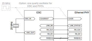
From the F29H85X controlSOM Evaluation Board user's guide:


The same Clock source choice is highlighted in the F29H85x and F29P58x Real-Time Microcontrollers Technical Reference Manual
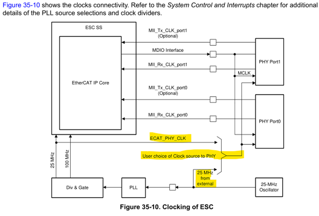
From the same section, the only warning about clocks is given:
[Quick note, I'm assuming:
ESC_PHY_CLK
ESCSS_PHY_CLK
ECAT_PHY_CLK
are all designating the same signal with conflicting names]
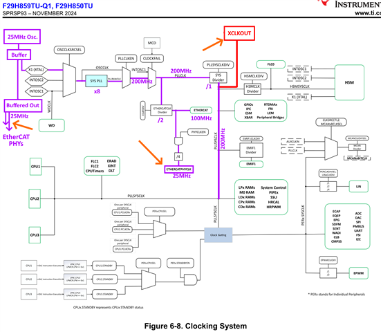
Also, there could be another way: XCLKOUT.
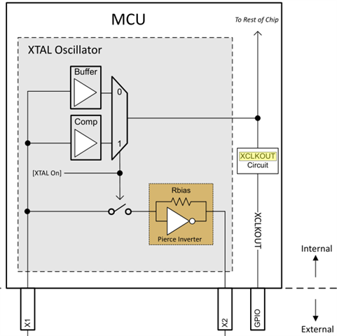
Configuring XCLKOUT with 1:1 with a 25MHz crystal would give a buffered 25MHz out.
=====
Now the questions:
There is ONE ESC_PHY_CLK signal, is it possible to output it on two GPIOs at the same time to feed both PHYs? (GPIO48 & GPIO54)
Or is it better to output on only one pin and route to the input of both PHYs? (Like on the EVM, where GPIO54 is used for both)
Does using ESC_PHY_CLK offer any difference from using XCLKOUT for the same function?
How can we evaluate the drawbacks from using those instead of an external clock buffer?
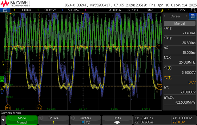
Is the Jitter and Delay added by using ESC_PHY_CLK or XCLKOUT specified for the F29H850TU?
On one hand I am told "this pin is for that", on the other "but you better not use it"... just a bit confused.
Thanks!


