Tool/software:
Hello TI Team,
I am using the TMS320F28377S and trying to establish communication using the SPI module. I’ve been working on this for two days but haven’t been able to get it working properly.
When I write my own SPI communication functions without making any changes to the configuration, I am able to write and read data successfully.
The device I am trying to communicate with is an EEPROM chip: 25LC640A-E/SN. Could you please help me with this?
Below are the pin assignments and the code I have prepared.
(Nonfunctional)
void SPI_GPIO_Init(void)
{
EALLOW;

// === MOSI: GPIO24 → SPISIMOB ===
GpioCtrlRegs.GPAGMUX2.bit.GPIO24 = 1; // Set GPIO24 to use GMUX option 1
GpioCtrlRegs.GPAMUX2.bit.GPIO24 = 2; // Set MUX to 2 for SPISIMOB function
GpioCtrlRegs.GPAQSEL2.bit.GPIO24 = 3;

// === MISO: GPIO25 → SPISOMIB ===
GpioCtrlRegs.GPAGMUX2.bit.GPIO25 = 1; // Set GPIO25 to use GMUX option 1
GpioCtrlRegs.GPAMUX2.bit.GPIO25 = 2; // Set MUX to 2 for SPISOMIB function
GpioCtrlRegs.GPAQSEL2.bit.GPIO25 = 3;

// === CLK: GPIO26 → SPICLKB ===
GpioCtrlRegs.GPAGMUX2.bit.GPIO26 = 1; // Set GPIO26 to use GMUX option 1
GpioCtrlRegs.GPAMUX2.bit.GPIO26 = 2; // Set MUX to 2 for SPICLKB function
GpioCtrlRegs.GPAQSEL2.bit.GPIO26 = 3;

// === Set GPIO directions ===
GpioCtrlRegs.GPADIR.bit.GPIO24 = 1; // MOSI: output
GpioCtrlRegs.GPADIR.bit.GPIO25 = 0; // MISO: input
GpioCtrlRegs.GPADIR.bit.GPIO26 = 1; // CLK: output

// === Enable internal pull-up resistors ===
GpioCtrlRegs.GPAPUD.bit.GPIO24 = 0; // Enable pull-up for MOSI
GpioCtrlRegs.GPAPUD.bit.GPIO25 = 0; // Enable pull-up for MISO
GpioCtrlRegs.GPAPUD.bit.GPIO26 = 0; // Enable pull-up for CLK

GpioCtrlRegs.GPBMUX1.bit.GPIO38 = 0; // Set GPIO38 to GPIO function
GpioCtrlRegs.GPBDIR.bit.GPIO38 = 1; // Set as output
GpioCtrlRegs.GPBPUD.bit.GPIO38 = 0; // Enable pull-up resistor
GpioDataRegs.GPBSET.bit.GPIO38 = 1; // Set HIGH initially (inactive)

EDIS;
}


void SPI_INIT()
{

EALLOW;
GpioDataRegs.GPBSET.bit.GPIO38 = 1; // nCS HIGH


CpuSysRegs.PCLKCR8.bit.SPI_B = 1;
SpibRegs.SPICCR.bit.SPISWRESET = 0; // Reset SPI
SpibRegs.SPICCR.bit.CLKPOLARITY = 0; // Clock polarity 0
SpibRegs.SPICTL.bit.CLK_PHASE = 0 ;
SpibRegs.SPICCR.bit.SPICHAR = 7; // 8-bit data
SpibRegs.SPICTL.bit.MASTER_SLAVE = 1; // Master mode
SpibRegs.SPICTL.bit.TALK = 1; // TX enable
SpibRegs.SPIBRR.bit.SPI_BIT_RATE = 21; // Baud Rate
SpibRegs.SPICCR.bit.SPISWRESET = 1; // Release SPI from reset

EDIS;

}

void EEPROM_WriteByte(Uint16 address, Uint8 data)
{
// Write Enable
GpioDataRegs.GPBCLEAR.bit.GPIO38 = 1; // nCS LOW
SPIB_SendByte(0x06); // Write Enable opcode
GpioDataRegs.GPBSET.bit.GPIO38 = 1; // nCS HIGH

// Write Command
SPI_Delay();
GpioDataRegs.GPBCLEAR.bit.GPIO38 = 1;

SPIB_SendByte(0x02); // WRITE opcode
SPIB_SendByte((address >> 8) & 0xFF); // Address High Byte
SPIB_SendByte(address & 0xFF); // Address Low Byte
SPIB_SendByte(data); // Data byte

GpioDataRegs.GPBSET.bit.GPIO38 = 1;

DELAY_US(5000); // Wait write cycle (max 5ms)
}

Uint8 EEPROM_ReadByte(Uint16 address)
{
Uint8 value;

GpioDataRegs.GPBCLEAR.bit.GPIO38 = 1;

SPIB_SendByte(0x03); // READ opcode
SPIB_SendByte((address >> 8) & 0xFF); // Address High Byte
SPIB_SendByte(address & 0xFF); // Address Low Byte
value = SPIB_SendByte(0x00); // Dummy write to receive data


DELAY_US(5);
GpioDataRegs.GPBSET.bit.GPIO38 = 1;

return value;
}

Uint16 SPIB_SendByte(Uint16 data)
{
while (SpibRegs.SPISTS.bit.BUFFULL_FLAG == 1); // Wait if TX buffer full
SpibRegs.SPITXBUF = data << 8;

while (SpibRegs.SPISTS.bit.INT_FLAG == 0); // Wait for RX
return SpibRegs.SPIRXBUF & 0x00FF;
}

void SPI_Delay(void)
{
asm(" RPT #50 || NOP");
}
I tested in the main loop
void main(void)
{
    for(;;)
    {
        if(spi_write_test==1)
        {
            EEPROM_WriteByte(0x1234, 0xAA);
            spi_write_test=0;
        }

        if(spi_read_test==1)
        {
            EEPROM_ReadByte(0x1234);
            spi_read_test=0;
        }
    }
}
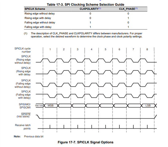
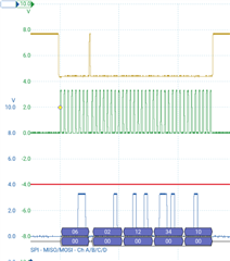
Clock Frequency --> 750kHz
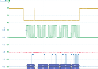
Write sequence
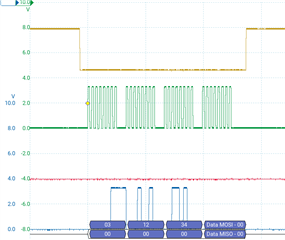
Read Sequence
(Functional)
void SPI_GPIO_Init(void)
{
    EALLOW;

    // MOSI (Master Out, Slave In) -> GPIO24
    GpioCtrlRegs.GPAMUX2.bit.GPIO24 = 0; // Set as GPIO
    GpioCtrlRegs.GPADIR.bit.GPIO24 = 1;  // Configure as output

    // MISO (Master In, Slave Out) -> GPIO25
    GpioCtrlRegs.GPAMUX2.bit.GPIO25 = 0; // Set as GPIO
    GpioCtrlRegs.GPADIR.bit.GPIO25 = 0;  // Configure as input

    // CLK (Clock) -> GPIO26
    GpioCtrlRegs.GPAMUX2.bit.GPIO26 = 0; // Set as GPIO
    GpioCtrlRegs.GPADIR.bit.GPIO26 = 1;  // Configure as output

    // CS (Chip Select) -> GPIO38
    GpioCtrlRegs.GPBMUX1.bit.GPIO38 = 0; // Set as GPIO
    GpioCtrlRegs.GPBDIR.bit.GPIO38 = 1;  // Configure as output

    EDIS;
}


void SPI_Delay(void)
{
    asm(" RPT #50 || NOP"); // Short delay between clock transitions
}


void SPI_SendByte(uint8_t data)
{
    int i;

    for (i = 7; i >= 0; i--)
    {
        if ((data >> i) & 0x01)
            GpioDataRegs.GPASET.bit.GPIO24 = 1; // MOSI high
        else
            GpioDataRegs.GPACLEAR.bit.GPIO24 = 1; // MOSI low

        SPI_Delay();

        GpioDataRegs.GPASET.bit.GPIO26 = 1; // CLK high
        SPI_Delay();

        GpioDataRegs.GPACLEAR.bit.GPIO26 = 1; // CLK low
        SPI_Delay();
    }
}


uint8_t SPI_ReadByte(void)
{
    int i;
    uint8_t received = 0;

    for (i = 7; i >= 0; i--)
    {
        // Dummy 0 bit on MOSI
        GpioDataRegs.GPACLEAR.bit.GPIO24 = 1;

        SPI_Delay();

        GpioDataRegs.GPASET.bit.GPIO26 = 1; // CLK high
        SPI_Delay();

        // Sample MISO
        if (GpioDataRegs.GPADAT.bit.GPIO25)
            received |= (1 << i);

        GpioDataRegs.GPACLEAR.bit.GPIO26 = 1; // CLK low
        SPI_Delay();
    }

    return received;
}


void EEPROM_Write_0x1234_0x10(void)
{
    // Step 1: Send WREN command (Write Enable)
    GpioDataRegs.GPBCLEAR.bit.GPIO38 = 1; // CS low
    SPI_SendByte(0x06); // WREN command
    GpioDataRegs.GPBSET.bit.GPIO38 = 1;   // CS high
    SPI_Delay(); // Small delay if needed

    // Step 2: Send WRITE command + Address + Data
    GpioDataRegs.GPBCLEAR.bit.GPIO38 = 1; // CS low

    SPI_SendByte(0x02);   // WRITE command
    SPI_SendByte(0x12);   // Address MSB (0x12 for 0x1234)
    SPI_SendByte(0x34);   // Address LSB (0x34 for 0x1234)
    SPI_SendByte(0xAA);   // Data byte (0x10)

    GpioDataRegs.GPBSET.bit.GPIO38 = 1;   // CS high

    // Step 3: Wait for write cycle to complete (typical 5ms)
    DELAY_US(5000); // 5 milliseconds wait
}


uint8_t EEPROM_Read_0x1234(void)
{
    uint8_t read_data;

    GpioDataRegs.GPBCLEAR.bit.GPIO38 = 1; // CS low - start communication

    SPI_SendByte(0x03);   // READ command
    SPI_SendByte(0x12);   // Address MSB
    SPI_SendByte(0x40);   // Address LSB

    read_data = SPI_ReadByte(); // Read one byte

    GpioDataRegs.GPBSET.bit.GPIO38 = 1;   // CS high - end communication

    return read_data;
}
Main Loop
void main(void)
{
    for(;;)
    {
        if(spi_write_test==1)
        {
            EEPROM_Write_0x1234_0x10();
            spi_write_test=0;
        }

        if(spi_read_test==1)
        {
            EEPROM_Read_0x1234();
            spi_read_test=0;
        }
    }
}
Write
Read
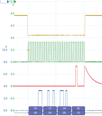
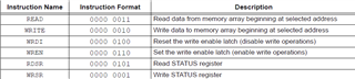
EEPROM Device command table