


Tool/software:
Hi experts
Question 1:
Feed two analog signals to ADCINA2 and ADCINA4, and generate two EVT events via the internal comparator of the chip to synchronize the frequency conversion of PWM3 and PWM5 respectively. Additionally, the sync event for PWM3 synchronization is also used to trigger the capture of PWM5. The TBCTR of PWM5 at the PWM3 synchronization moment is captured via the DCCAP register. However, during actual operation, it was found that when configuring CAPE for this PWM5, the waveform fails to pull down normally during generation, resulting in abnormal sawtooth waveforms as shown below:
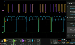
Among them, channels CH1 and CH2 show the PWM3 waveforms without CAPE enable configuration, while channels CH2 and CH4 display the PWM5 waveforms after capture configuration., the normal waveform should be consistent with that of CH3. The waveform was tested at the chip's PWM output port, with the subsequent power drive circuit disconnected to avoid interfering with the chip's drive.
Question 2:
Use HRCAP for PWM period capture. Connect PWM3B on pin 50 to HRCAP2 on pin 60 to acquire the PWM period, and enable the RISE interrupt for HRCAP2. The main interrupt is configured by PWM7 to a fixed 100kHz. During actual use, the following issues occur:

(1) The RISE interrupt has an inconsistent delay of several microseconds compared to the transition time of the rising edge captured by pin 50. According to the datasheet, it should be at most around ten clock cycles (with a main clock frequency of 60MHz). Why is this happening?
(2) Since PWM3B has a variable frequency ranging from 20kHz to 500kHz, when the main interrupt and HRCAP interrupt are triggered simultaneously, the HRCAP interrupt exits abnormally. It is uncertain whether the captured period value remains normal during abnormal exit.
In the main interrupt and HRCAP interrupt, toggle signals are configured respectively. In the main interrupt, CH3 signal is set high upon entry and low upon exit. The HRCAP toggle signal uses TOGGLE mode, setting it high in the current interrupt and low in the next. The toggle signals for both interrupts are configured with PWM6 in immediate mode, using the AQCSFRC register for forced toggling to reflect the interrupt entry/exit timing as quickly as possible.
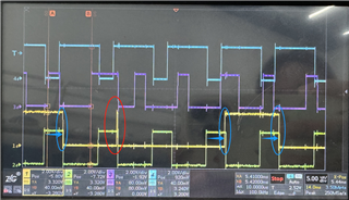
CH2 is PWM3B, CH1 is the toggle signal for HRCAP interrupt, and CH3 is the toggle signal for the main interrupt.
As shown in the figure above, the area circled in blue indicates the HRCAP interrupt entry moment, which is delayed by several microseconds compared to the actual PWM3B drive edge. The area circled in red shows the abnormal exit moment of the HRCAP interrupt: when the HRCAP interrupt and main interrupt are triggered simultaneously, the HRCAP interrupt exits abnormally. At this time, the interval between two adjacent main interrupts deviates from 100kHz, but their combined period equals 50kHz. The crystal oscillator frequency at this moment has been verified to be normal.
(3) When an 800mV interference signal exists on PWM3B, the capture accuracy is compromised (verified by power supply, single-board, and signal generator). The datasheet does not specify the description of rising/falling edge levels for capture. What are the actual signal quality requirements for PWM3B when using HRCAP for capture?
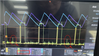
CH2 is the capture signal fed into the HRCAP2 pin, and noise signals will cause capture inaccuracies.
(4) To avoid preemption between HRCAP interrupt and the main interrupt, if HRCAP interrupt is not configured, and the PWM3 period value is directly calculated in the main interrupt as TPR = (HRCap2Regs.HCCAPCNTFALL0 + HRCap2Regs.HCCAPCNTRISE0 + 1), will there be errors?
Question 3
When the pulse widths of COMP1OUT and COMP2OUT are several microseconds and partially overlap despite having a phase difference, the capture value of DCCAP is 1, making it impossible to obtain the phase difference.
The attachment contains PWM-related configurations for the above issues.
// B相桥臂高频管:对应硬件PWM3/PWM4发波配置
static void RtHal_Pwm3Cfg(void)
{
    // PWM3A和PWM3B配置
    EALLOW;
    EPwm3Regs.TBCTL.bit.HSPCLKDIV = TB_DIV1;              // 高速时钟预分频
    EPwm3Regs.TBCTL.bit.CLKDIV = TB_DIV1;                 // 时钟预分频
    EPwm3Regs.TBPRD = POWER_PWM_TPR;                      // 20kHz
    EPwm3Regs.TBPHS.half.TBPHS = 0;                       // 同步事件发生时相位从0开始加载
    EPwm3Regs.TBCTL.bit.CTRMODE = TB_COUNT_UP;            // up计数模式
    EPwm3Regs.TBCTL.bit.PHSEN = TB_ENABLE;                // 当发生EPWMxSYNCI同步事件时,从TBPHS加载时基计数。

    EPwm3Regs.TBCTL.bit.PRDLD = TB_SHADOW;
    EPwm3Regs.TBCTL.bit.SYNCOSEL = TB_SYNC_DISABLE;       // 不生成EPWMxSYNCO信号
    EPwm3Regs.CMPCTL.bit.SHDWAMODE = TB_SHADOW;           // shadow
    EPwm3Regs.CMPCTL.bit.SHDWBMODE = TB_SHADOW;           // shadow
    EPwm3Regs.CMPCTL.bit.LOADAMODE = CC_CTR_ZERO;         // load on CTR=Zero
    EPwm3Regs.CMPCTL.bit.LOADBMODE = CC_CTR_ZERO;         // load on CTR=Zero

    EPwm3Regs.AQCTLA.bit.CAU = AQ_SET;
    EPwm3Regs.AQCTLA.bit.CBU = AQ_CLEAR;

    EPwm3Regs.TZCTL.bit.TZA = TZ_FORCE_LO;    // IFY建议
    EPwm3Regs.TZCTL.bit.TZB = TZ_FORCE_LO;

    // DCAH和DCBH配置
    EPwm3Regs.DCTRIPSEL.bit.DCAHCOMPSEL = DC_COMP2OUT;    // DCAH
    EPwm3Regs.TZDCSEL.bit.DCAEVT1 = TZ_DCAH_HI;           // DCAH = high, DCAL = don't care
    EPwm3Regs.DCACTL.bit.EVT1SRCSEL = DC_EVT_DIS_FLT;     // DCAEVT1事件不滤波
    EPwm3Regs.DCACTL.bit.EVT1FRCSYNCSEL = DC_EVT_SYNC;    // DCAEVT1 Force Synchronization Signal Select:0 同步信号
    EPwm3Regs.DCACTL.bit.EVT1SYNCE = 1;                   // 1:SYNC Generation Enabled (DCAEVT1.sync)
    EPwm3Regs.TZCTL.bit.DCAEVT1 = TZ_NO_CHANGE;

    EPwm3Regs.DCTRIPSEL.bit.DCBHCOMPSEL = DC_COMP2OUT;    // DCBH
    EPwm3Regs.TZDCSEL.bit.DCBEVT2 = TZ_DCBH_HI;           // DCBEVT1用于配置COMP3-OST保护,所以此处用DCBEVT2
    EPwm3Regs.DCBCTL.bit.EVT2SRCSEL = DC_EVT_DIS_FLT;     // DCBEVT2事件不滤波
    EPwm3Regs.DCBCTL.bit.EVT2FRCSYNCSEL = DC_EVT_SYNC;
    EPwm3Regs.TZCTL.bit.DCBEVT2 = TZ_NO_CHANGE;

    // 死区配置
    EPwm3Regs.DBCTL.bit.OUT_MODE = DB_FULL_ENABLE;        // enable Dead-band module
    EPwm3Regs.DBCTL.bit.POLSEL = DB_ACTV_HIC;             // Active Hi complementary
    EPwm3Regs.DBFED = 42;
    EPwm3Regs.DBRED = 42;
    EPwm3Regs.CMPA.half.CMPA = 0;
    EPwm3Regs.CMPB = 1500;
    EDIS;
}


// A相桥臂高频管发波配置
static void RtHal_Pwm5Cfg(void)
{
    EALLOW;
    EPwm5Regs.TBCTL.bit.HSPCLKDIV = TB_DIV1;              // 高速时钟预分频
    EPwm5Regs.TBCTL.bit.CLKDIV = TB_DIV1;                 // 时钟预分频
    EPwm5Regs.TBPRD = POWER_PWM_TPR;                      // 20kHz
    EPwm5Regs.TBPHS.half.TBPHS = 0;                       // 同步事件发生时相位从0开始加载
    EPwm5Regs.TBCTL.bit.CTRMODE = TB_COUNT_UP;            // up计数模式
    EPwm5Regs.TBCTL.bit.PHSEN = TB_ENABLE;                // 当发生EPWMxSYNCI同步事件时,从TBPHS加载时基计数。

    EPwm5Regs.TBCTL.bit.PRDLD = TB_SHADOW;
    EPwm5Regs.TBCTL.bit.SYNCOSEL = TB_SYNC_DISABLE;       // 不生成EPWMxSYNCO信号
    EPwm5Regs.CMPCTL.bit.SHDWAMODE = TB_SHADOW;           // shadow
    EPwm5Regs.CMPCTL.bit.SHDWBMODE = TB_SHADOW;           // shadow
    EPwm5Regs.CMPCTL.bit.LOADAMODE = CC_CTR_ZERO;         // load on CTR=Zero
    EPwm5Regs.CMPCTL.bit.LOADBMODE = CC_CTR_ZERO;         // load on CTR=Zero

    EPwm5Regs.AQCTLA.bit.CAU = AQ_SET;                    // 正半周期 5A为辅助管
    EPwm5Regs.AQCTLA.bit.CBU = AQ_CLEAR;                  // 正半周期 5B为主管

    EPwm5Regs.TZCTL.bit.TZA = TZ_FORCE_LO;                // IFY建议 可以解决OST封波拖尾问题
    EPwm5Regs.TZCTL.bit.TZB = TZ_FORCE_LO;

    // DCAH和DCBH选择
    EPwm5Regs.DCTRIPSEL.bit.DCAHCOMPSEL = DC_COMP1OUT;    // DCAH:COMP1OUT input
    EPwm5Regs.TZDCSEL.bit.DCAEVT1 = TZ_DCAH_HI;           // DCAH = high, DCAL = don't care
    EPwm5Regs.DCACTL.bit.EVT1SRCSEL = DC_EVT_DIS_FLT;     // DCAEVT1事件不滤波
    EPwm5Regs.DCACTL.bit.EVT1FRCSYNCSEL = DC_EVT_SYNC;    // DCAEVT1 Force Synchronization Signal Select:0 同步信号
    EPwm5Regs.DCACTL.bit.EVT1SYNCE = 1;                   // 1:使能DCAEVT1.sync
    EPwm5Regs.TZCTL.bit.DCAEVT1 = TZ_NO_CHANGE;            // 数字比较事件强制EPWM5A为低电平

    EPwm5Regs.DCTRIPSEL.bit.DCBHCOMPSEL = DC_COMP1OUT;    // DCBH:COMP1OUT input
    EPwm5Regs.TZDCSEL.bit.DCBEVT2 = TZ_DCBH_HI;           // DCBH = high, DCBL = don't care
    EPwm5Regs.DCBCTL.bit.EVT2SRCSEL = DC_EVT_DIS_FLT;     // DCBEVT1事件不滤波
    EPwm5Regs.DCBCTL.bit.EVT2FRCSYNCSEL = DC_EVT_SYNC;    // DCAEVT1 Force Synchronization Signal Select:0 同步信号
    EPwm5Regs.TZCTL.bit.DCBEVT2 = TZ_NO_CHANGE;            // 数字比较事件强制EPWM5B为低电平

     // 计数锁存配置
    EPwm5Regs.DCTRIPSEL.bit.DCALCOMPSEL = DC_COMP1OUT;    // pwm5变频的触发源DCAL用于捕获
    EPwm5Regs.TZDCSEL.bit.DCAEVT2 = TZ_DCAL_HI;           // DCBEVT1用于配置COMP3-OST保护,所以此处用DCBEVT2
    EPwm5Regs.DCACTL.bit.EVT2SRCSEL = DC_EVT_DIS_FLT;     // DCBEVT2事件不滤波
    EPwm5Regs.DCACTL.bit.EVT2FRCSYNCSEL = DC_EVT_SYNC;

    EPwm5Regs.DCCAPCTL.bit.CAPE = 1;                      // 1:使能捕获
    EPwm5Regs.DCCAPCTL.bit.SHDWMODE = 0;                  // 1:Active Mode   0:shadow mode
    EPwm5Regs.DCFCTL.bit.PULSESEL = DC_PULSESEL_ZERO;     // TBCTR=TPR前捕获事件将被忽略  0x01为TBCTR=0
    EPwm5Regs.DCFCTL.bit.SRCSEL = DC_SRC_DCAEVT2;         // 选择为DCAEVT2信号为捕获触发事件
    EPwm5Regs.DCFCTL.bit.BLANKE = DC_BLANK_DISABLE;       // 禁能消隐窗口(一直高电平)


    // 死区配置
    EPwm5Regs.DBCTL.bit.OUT_MODE = DB_FULL_ENABLE;        // enable Dead-band module
    EPwm5Regs.DBCTL.bit.POLSEL = DB_ACTV_HIC;             // Active Hi complementary
    EPwm5Regs.DBFED = 42;                                 // 下降沿延迟FED = 50 TBCLKs
    EPwm5Regs.DBRED = 42;                                 // 上升沿延迟RED = 50 TBCLKs
    EPwm5Regs.CMPA.half.CMPA = 0;
    EPwm5Regs.CMPB = 1500;
    EDIS;
}


void InitComp(void)
{
    // 数字比较器COMP1配置,用于同步A相桥臂PWM5
    EALLOW;
    AdcRegs.ADCCTL1.bit.ADCBGPWD = 1;       // 低功耗时关闭,其它时候打开确保ADC基准供电正常
    Comp1Regs.DACCTL.bit.DACSOURCE = 0;     // Select DACVAL to control the DAC.
    Comp1Regs.COMPCTL.bit.COMPSOURCE = 0;   // comp-B端输入:internal DAC即比较器ref.
    Comp1Regs.COMPCTL.bit.SYNCSEL = 1;      // 比较结果同步还是异步输出:0:异步(传输延迟小、不稳定)1:同步(与系统时钟同步):稳定、可靠
    Comp1Regs.COMPCTL.bit.COMPDACEN = 1;    // Comparator/DAC Enable
    Comp1Regs.COMPCTL.bit.QUALSEL = 2;
    Comp1Regs.DACVAL.bit.DACVAL = 493;      // bit0-9:DAC Value bits, scales the output of the DAC from 0~1023
    Comp1Regs.COMPCTL.bit.CMPINV = 1;       // 比较器结果:IL>DACVAL→高电平

    // 数字比较器COMP2配置,用于同步B相桥臂PWM3
    Comp2Regs.DACCTL.bit.DACSOURCE = 0;     // Select DACVAL to control the DAC.
    Comp2Regs.COMPCTL.bit.COMPSOURCE = 0;   // comp-B端输入:internal DAC即比较器ref.
    Comp2Regs.COMPCTL.bit.SYNCSEL = 1;      // 比较结果同步还是异步输出:0:异步(传输延迟小、不稳定)1:同步(与系统时钟同步):稳定、可靠
    Comp2Regs.COMPCTL.bit.COMPDACEN = 1;    // Comparator/DAC Enable
    Comp2Regs.COMPCTL.bit.QUALSEL = 2;
    Comp2Regs.DACVAL.bit.DACVAL = 493;      // bit0-9:DAC Value bits, scales the output of the DAC from 0~1023
    Comp2Regs.COMPCTL.bit.CMPINV = 1;       // 比较器结果:IL>DACVAL→高电平

    // 数字比较器COMP3配置,用于封波
    Comp3Regs.DACCTL.bit.DACSOURCE = 0;     // Select DACVAL to control the DAC.
    Comp3Regs.COMPCTL.bit.COMPSOURCE = 0;   // comp-B端输入:internal DAC即比较器ref.
    Comp3Regs.COMPCTL.bit.SYNCSEL = 1;      // 比较结果同步还是异步输出:0:异步(传输延迟小、不稳定)1:同步(与系统时钟同步):稳定、可靠
    Comp3Regs.COMPCTL.bit.COMPDACEN = 1;    // Comparator/DAC Enable
    // 电网电压正半周时:
    Comp3Regs.DACVAL.bit.DACVAL = 735;      // bit0-9:DAC Value bits, scales the output of the DAC from 0~1023
    Comp3Regs.COMPCTL.bit.CMPINV = 0;       // 比较器结果:IL>DACVAL→高电平
    EDIS;
}


// 以下函数根据电网正负半周期进行切换
#define NEG_IN_COMP_CFG()                            \
   do {                                              \
           EALLOW;                                   \
           Comp1Regs.DACVAL.bit.DACVAL = (g_offsetCalc.IinA_Negoffset - 28);        \
           Comp1Regs.COMPCTL.bit.CMPINV = 1;         \
           Comp2Regs.DACVAL.bit.DACVAL = (g_offsetCalc.IinB_Negoffset - 28);        \
           Comp2Regs.COMPCTL.bit.CMPINV = 1;         \
           Comp3Regs.DACVAL.bit.DACVAL = 735;        \
           Comp3Regs.COMPCTL.bit.CMPINV = 0;         \
           EPwm3Regs.DBFED = 18;                     \
           EPwm3Regs.DBRED = 33;                     \
           EPwm5Regs.DBFED = 18;                     \
           EPwm5Regs.DBRED = 33;                     \
           EDIS;                                     \
   } while(0)


// 电网电压正半周时:模拟比较器配置  A comp1
// COMP1、2:正负半周期>2A -> 1.71V -> DACVAL= 530
// COMP1、2:正半周期>1.5A -> 1.695V -> DACVAL= 525
// COMP1、2:正半周期>1A -> 1.68V -> DACVAL= 521
// COMP1、2:正半周期>0.5A -> 1.665V -> DACVAL= 516
// COMP3:rms=20A对应<0.9288 -> 288         //  +COMP2  23

#define POS_IN_COMP_CFG()                            \
   do {                                              \
           EALLOW;                                   \
           Comp1Regs.DACVAL.bit.DACVAL = (g_offsetCalc.IinA_Posoffset + 28);        \
           Comp1Regs.COMPCTL.bit.CMPINV = 0;         \
           Comp2Regs.DACVAL.bit.DACVAL = (g_offsetCalc.IinB_Posoffset + 28);        \
           Comp2Regs.COMPCTL.bit.CMPINV = 0;         \
           Comp3Regs.DACVAL.bit.DACVAL = 288;        \
           Comp3Regs.COMPCTL.bit.CMPINV = 1;         \
           EPwm3Regs.DBFED = 33;                     \
           EPwm3Regs.DBRED = 18;                     \
           EPwm5Regs.DBFED = 33;                     \
           EPwm5Regs.DBRED = 18;                     \
           EDIS;                                     \
   } while(0)

