This thread has been locked.

If you have a related question, please click the "Ask a related question" button in the top right corner. The newly created question will be automatically linked to this question.

TMS320F28379D: Code not executing after a POR

Part Number: TMS320F28379D
Other Parts Discussed in Thread: UNIFLASH, LAUNCHXL-F28379D, C2000WARE, SYSCONFIG

Tool/software:

Hi Team,

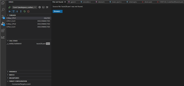
We are experiencing an issue where we observe that the code not executing after cutting off the power to the MCU and then giving it back again after sometime.

We have designed a custom board for our motor control application using TMS320F28379D. Currently we are powering it through the launchpad (LAUNCHXL f28379D) since our another board (Power board) which we have designed to power this custom board  has not arrived yet.

The code(firmware) that we have flashed is a simple LED blinking on our custom board.

So, we are investigating what could be the issue for this behaviour?

Could it be an Hardware issue or could it be a firmware issue ?

We would appreciate your help to identify the cause. Do let me know if you have any suggestions for us to check and verify in this design.

  • Hello Team,

    Could we have any update on this ?

  • Hi,

    Have you verified that the flash has been programmed and the MCU is booting to flash?

    Thanks,

    Ben Collier

  • Hi  ,

    Thanks a lot for your response.

    No, I have not verified that.

    How do I verify that  the flash has been programmed and the MCU is booting to flash.

    Could you please guide me with the required steps to do so?

  • Hi,

    You will need to connect to the device and check the flash locations in memory. 

    Also check your linker command file and make sure that the code is being placed in flash.

    Best Regards,

    Ben Collier

  • MEMORY
    {
    PAGE 0 :  /* Program Memory */
              /* Memory (RAM/FLASH) blocks can be moved to PAGE1 for data allocation */
              /* BEGIN is used for the "boot to Flash" bootloader mode   */
    
       BEGIN           	: origin = 0x080000, length = 0x000002
       RAMM0           	: origin = 0x000123, length = 0x0002DD
       RAMD0           	: origin = 0x00B000, length = 0x000800
       RAMLS0          	: origin = 0x008000, length = 0x000800
       RAMLS1          	: origin = 0x008800, length = 0x000800
       RAMLS2      		: origin = 0x009000, length = 0x000800
       RAMLS3      		: origin = 0x009800, length = 0x000800
       RAMLS4      		: origin = 0x00A000, length = 0x000800
       RAMGS14          : origin = 0x01A000, length = 0x001000     /* Only Available on F28379D, F28377D, F28375D devices. Remove line on other devices. */
       RAMGS15          : origin = 0x01B000, length = 0x000FF8     /* Only Available on F28379D, F28377D, F28375D devices. Remove line on other devices. */
    
    //   RAMGS15_RSVD     : origin = 0x01BFF8, length = 0x000008    /* Reserve and do not use for code as per the errata advisory "Memory: Prefetching Beyond Valid Memory" */
    
       RESET           	: origin = 0x3FFFC0, length = 0x000002
    
       /* Flash sectors */
       FLASHA           : origin = 0x080002, length = 0x001FFE	/* on-chip Flash */
       FLASHB           : origin = 0x082000, length = 0x002000	/* on-chip Flash */
       FLASHC           : origin = 0x084000, length = 0x002000	/* on-chip Flash */
       FLASHD           : origin = 0x086000, length = 0x002000	/* on-chip Flash */
       FLASHE           : origin = 0x088000, length = 0x008000	/* on-chip Flash */
       FLASHF           : origin = 0x090000, length = 0x008000	/* on-chip Flash */
       FLASHG           : origin = 0x098000, length = 0x008000	/* on-chip Flash */
       FLASHH           : origin = 0x0A0000, length = 0x008000	/* on-chip Flash */
       FLASHI           : origin = 0x0A8000, length = 0x008000	/* on-chip Flash */
       FLASHJ           : origin = 0x0B0000, length = 0x008000	/* on-chip Flash */
       FLASHK           : origin = 0x0B8000, length = 0x002000	/* on-chip Flash */
       FLASHL           : origin = 0x0BA000, length = 0x002000	/* on-chip Flash */
       FLASHM           : origin = 0x0BC000, length = 0x002000	/* on-chip Flash */
       FLASHN           : origin = 0x0BE000, length = 0x001FF0	/* on-chip Flash */
    
    //   FLASHN_RSVD     : origin = 0x0BFFF0, length = 0x000010    /* Reserve and do not use for code as per the errata advisory "Memory: Prefetching Beyond Valid Memory" */
    
    PAGE 1 : /* Data Memory */
             /* Memory (RAM/FLASH) blocks can be moved to PAGE0 for program allocation */
    
       BOOT_RSVD       : origin = 0x000002, length = 0x000121     /* Part of M0, BOOT rom will use this for stack */
       RAMM1           : origin = 0x000400, length = 0x0003F8     /* on-chip RAM block M1 */
    //   RAMM1_RSVD      : origin = 0x0007F8, length = 0x000008     /* Reserve and do not use for code as per the errata advisory "Memory: Prefetching Beyond Valid Memory" */
       RAMD1           : origin = 0x00B800, length = 0x000800
    
       RAMLS5      : origin = 0x00A800, length = 0x000800
    
       RAMGS0      : origin = 0x00C000, length = 0x001000
       RAMGS1      : origin = 0x00D000, length = 0x001000
       RAMGS2      : origin = 0x00E000, length = 0x001000
       RAMGS3      : origin = 0x00F000, length = 0x001000
       RAMGS4      : origin = 0x010000, length = 0x001000
       RAMGS5      : origin = 0x011000, length = 0x001000
       RAMGS6      : origin = 0x012000, length = 0x001000
       RAMGS7      : origin = 0x013000, length = 0x001000
       RAMGS8      : origin = 0x014000, length = 0x001000
       RAMGS9      : origin = 0x015000, length = 0x001000
       RAMGS10     : origin = 0x016000, length = 0x001000
    
    //   RAMGS11     : origin = 0x017000, length = 0x000FF8   /* Uncomment for F28374D, F28376D devices */
    
    //   RAMGS11_RSVD : origin = 0x017FF8, length = 0x000008    /* Reserve and do not use for code as per the errata advisory "Memory: Prefetching Beyond Valid Memory" */
    
       RAMGS11     : origin = 0x017000, length = 0x001000     /* Only Available on F28379D, F28377D, F28375D devices. Remove line on other devices. */
       RAMGS12     : origin = 0x018000, length = 0x001000     /* Only Available on F28379D, F28377D, F28375D devices. Remove line on other devices. */
       RAMGS13     : origin = 0x019000, length = 0x001000     /* Only Available on F28379D, F28377D, F28375D devices. Remove line on other devices. */
    
       CPU2TOCPU1RAM   : origin = 0x03F800, length = 0x000400
       CPU1TOCPU2RAM   : origin = 0x03FC00, length = 0x000400
    }
    
    SECTIONS
    {
       /* Allocate program areas: */
       .cinit              : > FLASHC      PAGE = 0, ALIGN(8)
       .text               : >> FLASHB | FLASHC | FLASHD | FLASHE      PAGE = 0, ALIGN(8)
       codestart           : > BEGIN       PAGE = 0, ALIGN(8)
       /* Allocate uninitalized data sections: */
       .stack              : > RAMM1       PAGE = 1
       .switch             : > FLASHC      PAGE = 0, ALIGN(8)
       .reset              : > RESET,      PAGE = 0, TYPE = DSECT /* not used, */
    
    #if defined(__TI_EABI__)
       .init_array         : > FLASHB,       PAGE = 0,       ALIGN(8)
       .bss                : > RAMLS5,       PAGE = 1
       .bss:output         : > RAMLS3,       PAGE = 0
       .bss:cio            : > RAMLS5,       PAGE = 1
       .data               : > RAMLS5,       PAGE = 1
       .sysmem             : > RAMLS5,       PAGE = 1
       /* Initalized sections go in Flash */
       .const              : > FLASHF,       PAGE = 0,       ALIGN(8)
    #else
       .pinit              : > FLASHB,       PAGE = 0,       ALIGN(8)
       .ebss               : >> RAMLS5 | RAMGS0 | RAMGS1,    PAGE = 1
       .esysmem            : > RAMLS5,       PAGE = 1
       .cio                : > RAMLS5,       PAGE = 1
       /* Initalized sections go in Flash */
       .econst             : >> FLASHF      PAGE = 0, ALIGN(8)
    #endif
    
       Filter_RegsFile     : > RAMGS0,	   PAGE = 1
    
       SHARERAMGS0		: > RAMGS0,		PAGE = 1
       SHARERAMGS1		: > RAMGS1,		PAGE = 1
       SHARERAMGS2		: > RAMGS2,		PAGE = 1
       ramgs0           : > RAMGS0,     PAGE = 1
       ramgs1           : > RAMGS1,     PAGE = 1
    
    #ifdef __TI_COMPILER_VERSION__
        #if __TI_COMPILER_VERSION__ >= 15009000
            #if defined(__TI_EABI__)
                .TI.ramfunc : {} LOAD = FLASHD,
                                     RUN = RAMLS0,
                                     LOAD_START(RamfuncsLoadStart),
                                     LOAD_SIZE(RamfuncsLoadSize),
                                     LOAD_END(RamfuncsLoadEnd),
                                     RUN_START(RamfuncsRunStart),
                                     RUN_SIZE(RamfuncsRunSize),
                                     RUN_END(RamfuncsRunEnd),
                                     PAGE = 0, ALIGN(8)
            #else
                .TI.ramfunc : {} LOAD = FLASHD,
                                 RUN = RAMLS0,
                                 LOAD_START(_RamfuncsLoadStart),
                                 LOAD_SIZE(_RamfuncsLoadSize),
                                 LOAD_END(_RamfuncsLoadEnd),
                                 RUN_START(_RamfuncsRunStart),
                                 RUN_SIZE(_RamfuncsRunSize),
                                 RUN_END(_RamfuncsRunEnd),
                                 PAGE = 0, ALIGN(8)
            #endif
        #else
       ramfuncs            : LOAD = FLASHD,
                             RUN = RAMLS0,
                             LOAD_START(_RamfuncsLoadStart),
                             LOAD_SIZE(_RamfuncsLoadSize),
                             LOAD_END(_RamfuncsLoadEnd),
                             RUN_START(_RamfuncsRunStart),
                             RUN_SIZE(_RamfuncsRunSize),
                             RUN_END(_RamfuncsRunEnd),
                             PAGE = 0, ALIGN(8)
        #endif
    
    #endif
    
       /* The following section definitions are required when using the IPC API Drivers */
        GROUP : > CPU1TOCPU2RAM, PAGE = 1
        {
            PUTBUFFER
            PUTWRITEIDX
            GETREADIDX
        }
    
        GROUP : > CPU2TOCPU1RAM, PAGE = 1
        {
            GETBUFFER :    TYPE = DSECT
            GETWRITEIDX :  TYPE = DSECT
            PUTREADIDX :   TYPE = DSECT
        }
    
       /* The following section definition are for SDFM examples */
       Filter1_RegsFile : > RAMGS1,	PAGE = 1, fill=0x1111
       Filter2_RegsFile : > RAMGS2,	PAGE = 1, fill=0x2222
       Filter3_RegsFile : > RAMGS3,	PAGE = 1, fill=0x3333
       Filter4_RegsFile : > RAMGS4,	PAGE = 1, fill=0x4444
       Difference_RegsFile : >RAMGS5, 	PAGE = 1, fill=0x3333
    }
    
    /*
    //===========================================================================
    // End of file.
    //===========================================================================
    */
    

    Hi Ben,

    Thank you for your response.

    I have verified that my device's flash has been programmed through reading back the program memory of device using Uniflash, And I observe code stored in it from memory locations 0x082000 as mentioned in my 2837xD_FLASH_lnk_cou1.cmd file. Also attaching its entire content below for your reference.

    The observation that I see is once I connect the XDS 110 and program the device the code executes perfectly(Led blinking) and as soon as I provide a power cycle (OFF to ON) then I do not see code executing(Led blinking) 

    It seems like the issue is related to Booting. I suspect it is not booting properly or booting at a random location instead of the desired location.

    When I did some digging, I see that the GPIO pins 72 and 84 are related to Boot modes.

    In our configuration(custom board design) we have not used both these pins anywhere. And while comparing it with LAUNCHXL-F28379D we observe that the launchpad boots & executes code properly when : 

    (GPIO72=0, GPIO84=0,TRST=0  or  GPIO72=1, GPIO84=1,TRST=1  or  GPIO72=1, GPIO84=1,TRST=0  or  GPIO72=0, GPIO84=0,TRST=1

    Could you help us with to know whether this issue could be related to Booting and let us know how these pins should be configured and is there any other method to fix this issue through software without having the need to use these pins at all ?

    Do let us know about all the ways to fix this problem or if this issue could be related to something else then do point us in that direction.

    Thanks a lot for your guidance, much appreciated !! 

  • Hi,

    Could you check the ROM Code and Peripheral Booting section of the TRM? It is possible to change which pins are boot mode pins, or simply hardcode a boot mode. It is generally recommended to use a boot pin so that you have the option to not boot to FLASH in case certain debug steps are required.

    Also, please make sure you are aware of this info:  TMS320F28375D: how to force cpu2 to go into main after reset

    Best Regards,

    Ben Collier

  • Hi Ben,

    Thank you for your response.

    We did found out the issue, apparently it was boot pins. After pulling GPIO72 & 84 high in our custom board design we saw the device booting properly after POR and executing code.

    Additionally, I have a question, In our design we have already used GPIO 84 for some other purpose so wanted to know if by reprogramming/choosing some different pins as boot pins through BOOTCTRL register will we be ale to change the boot mode to some other mode only once ? What else do we need to take care of while doing this? 

    Also we wanted to know, In future when we design our custom Bootloader how should these pins be configured, what should the boot mode be? Will it create any complications in this regards ? 

    Thank you.

  • Hi,

    In our design we have already used GPIO 84 for some other purpose so wanted to know if by reprogramming/choosing some different pins as boot pins through BOOTCTRL register will we be ale to change the boot mode to some other mode only once ? What else do we need to take care of while doing this? 

    You will be able to select new boot pins once, and you will be able to select between different boot modes as many times as you want by changing the state of the new boot pins at powerup. 

    Also we wanted to know, In future when we design our custom Bootloader how should these pins be configured, what should the boot mode be? Will it create any complications in this regards ? 

    Please tell me about your custom bootloader. 

    Best Regards,

    Ben Collier

  • Hi Ben,

    Thanks for your response.

    We haven't decided the architecture of our custom bootloader yet but it will be a CAN based bootloader(we will be using CAN to transfer the image/binary application file from the tool to the bootloader). It could be UART based too based on complexities that we face while developing.

    Also, We haven't used any external pullups in our design on these two gpios, can we use the internal pullups [GPIO_PIN_TYPE_PULLUP in GPIO_setPadConfig()] on these pins if available and use them to go into GET mode (Flash boot mode on default on unprogrammed device) ?

    Also can you point us to the resources/example code to change the BOOT mode through firmware using BOOTCTRL register, are there any steps that need to be followed while doing this?

  • Hi,

    Also, We haven't used any external pullups in our design on these two gpios, can we use the internal pullups [GPIO_PIN_TYPE_PULLUP in GPIO_setPadConfig()] on these pins if available and use them to go into GET mode (Flash boot mode on default on unprogrammed device) ?

    You will need to use external pullup resistors if you want to use boot pins. For first time programming, you should be able to connect with floating boot pins, and then you will be able to program new boot pins if you wish. When the MCU is booting in the application, you must use external resistors if you choose to use boot pins. It is also acceptable to program a permanent bootmode. This is generally discouraged, especially if you are using code security. Depending on security settings, it may not be possible to connect to a device in flash boot mode. 

    Please see this app note for instructions: https://www.ti.com/lit/pdf/spracp8

    Best Regards,

    Ben Collier

  • Hi Ben, 

    Thank you for these insights.

    We are exploring to use GPIO 42 and 43 as Boot pins instead of 72 & 84. We are following the dcsm_security_tool example project imported from 

    Resource Explorer tab in the CCs IDE : c2000 real-time microcontrollers/Embedded Software/C2000Ware(6.00.00.00)/English/Devices/F2837XD/F28377D/Examples/Driverlib/cpu1/dcsm/dcsm_security_tool

    We have made below changes in the sysconfig file provided in that project:

    Now, once we test these changes, In debug mode we observe below error after executing the last line : LB _c_int00

    Observe below images:

    So, wanted to know why is this happening?

    Could you help us resolving this ?

    FYI: We are using LAUNCHXL-F28379D to test this reconfiguration of Boot pins change first then planning to implement it on our custom board based on the results. The pins 42, 43 aren't pulled up/high with a resistor to 3.3 yet.

  • Hi,

    Can you post a new thread for this issue? We assign these threads based on topic, and this is no longer my area of expertise. Since this is a new issue(not where we started), I think it would be best if you create a new thread about setting you custom boot pins with the DCSM tool.

    Best Regards,

    Ben Collier

  • Sure Ben,

    Thanks a lot of your help, much appreciated!!

    I'll do the needful.