This thread has been locked.

If you have a related question, please click the "Ask a related question" button in the top right corner. The newly created question will be automatically linked to this question.

LAUNCHXL-F28379D: TMS320F28379D hangs when running the debugger -- OK if array size is small

Part Number: LAUNCHXL-F28379D
Other Parts Discussed in Thread: C2000WARE

Tool/software:

Hello,

I need to store a large array in FLASH memory but I am finding that the debugger never reaches the initialized state where you hit the "Continue" blue button. Same story with directly programming the FLASH, it doesn't go through.

For example, this works:

const uint32_t g_adcDataStoreSize = 10e3;
#pragma DATA_SECTION(g_adcDataStore,"g_adcDataStore_DATA_SECT")
uint16_t g_adcDataStore[g_adcDataStoreSize] = {0};
 

GOOD!

~~~~~~~~~~~~~

This does not work:

const uint32_t g_adcDataStoreSize = 100e3;
#pragma DATA_SECTION(g_adcDataStore,"g_adcDataStore_DATA_SECT")
uint16_t g_adcDataStore[g_adcDataStoreSize] = {0};

BAD!

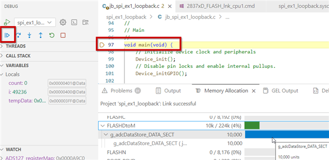
Left hanging, I never hit the "Resume" button and the code does not run. I know that the flash did not get written properly because I have a GPIO pin to set high as a test.

You can see in the picture there is plenty of space in FLASH memory, no build errors either.

Is there something improper in my .cmd file? Something else wrong?

.cmd file:

https://e2e.ti.com/cfs-file/__key/communityserver-discussions-components-files/171/2860.2837xD_5F00_FLASH_5F00_lnk_5F00_cpu1.cmd

.c file:

// #############################################################################
//
//  FILE:   spi_ex1_loopback.c
//
//  TITLE:  SPI Digital Loopback
//  [___ADC__]
//   Master out  |    GPIO63     |  H55 - yellow
//   Master in   |    GPIO64     |  H54 - green
//   CLK         |    GPIO65     |  H47 - red
//   CS          |    GPIO131    |  H58 - orange
//   TMR_SCP_OUT |    GPIO32     |  H2 - scope
//   TIMER_IN    |    GPIO40     |  H50 - from LMK5B
//   START       |    GPIO27     |  H52 - purple
//   RESET       |    GPIO25     |  H51 - blue
//   nDRDY_IN    |    GPIO15     |  H73 - unused
//   [__am64/ni spi__]
//   Master out  |    GPIO58     |  H15 -
//   Master in   |    GPIO59     |  H14 -
//   CLK         |    GPIO60     |  H7 -
//   CS          |    GPIO61     |  H19 - leave floating
//   Fake CS     |    GPIO125    |  H12 -  Use for 4-byte SPI
//   [__i2c ni__]
//   Master out  |    GPIO104     |  H9 - SCL
//   Master in   |    GPIO105    |  H10 - SDA

//! \addtogroup driver_example_list
//! <h1>SPI Digital Loopback</h1>
//!
//! This program uses the internal loopback test mode of the SPI module. This
//! is a very basic loopback that does not use the FIFOs or interrupts. A
//! stream of data is sent and then compared to the received stream.
//! The pinmux and SPI modules are configure through the sysconfig file.
//!
//! The sent data looks like this: \n
//!  0000 0001 0002 0003 0004 0005 0006 0007 .... FFFE FFFF 0000
//!
//! This pattern is repeated forever.
//!
//! \b External \b Connections \n
//!  - None
//!
//! \b Watch \b Variables \n
//!  - \b sData - Data to send
//!  - \b rData - Received data
//!
//
// #############################################################################
//
// Included Files
//
#include "ads127l21.h"

#include "board.h"
#include "device.h"
#include <math.h>
#include <stdio.h>
//#include "i2cLib_ex6_FIFO_master_interrupt.h"

//*******************************************************
//****************** FOR I2C ****************************
//*******************************************************
__interrupt void INT_ni_I2C_ISR(void){}
__interrupt void INT_ni_I2C_FIFO_ISR(void){}

//*******************************************************
//********* FOR TRIG from 5B ****************************
//*******************************************************
__interrupt void INT_TRIG_5B_IN_GPIO_XINT_ISR(void);

//*******************************************************
//****************** FOR ADC ****************************
//*******************************************************


const uint8_t g_adcDataBuffSize = 8; // data to average, set to powers of 2 for bitshift
int32_t g_adcDataBuff[g_adcDataBuffSize];   //raw data to be averaged, sampled as fast as possible

const uint32_t g_adcDataStoreSize = 100e3;//232e3; 
#pragma DATA_SECTION(g_adcDataStore,"g_adcDataStore_DATA_SECT")
uint16_t g_adcDataStore[g_adcDataStoreSize] = {0}; //averaged data, one every 10 kHz


uint8_t g_adcDataDiv;
int32_t g_adcDataSum;
int32_t g_adcDataAvg;
uint8_t g_adcCntBuff;
uint32_t g_adcCntStore;
bool g_endOfCapture;
uint8_t g_cnt = 0;


//
// Main
//
void main(void) {
    // Initialize device clock and peripherals
    Device_init();
    // Disable pin locks and enable internal pullups.
    Device_initGPIO();

    // Initialize PIE and clear PIE registers. Disables CPU interrupts.
    Interrupt_initModule();
    // Initialize the PIE vector table with pointers to the shell Interrupt
    // Service Routines (ISR).
    Interrupt_initVectorTable();

    // IMPORTANT: Make sure device is powered before setting GPIOs pins to HIGH
    // state. Initialize GPIOs pins used by ADS127L11 Initialize SPI peripheral
    // used by ADS127L11
    Board_init();
    ADS127_startUp();    

    volatile uint16_t count = 0;
    g_adcCntBuff = 0;
    g_adcCntStore = 0;
    g_adcDataDiv = log2(g_adcDataBuffSize);
    g_adcDataSum = 0;
    g_adcDataAvg = 0;  
    g_endOfCapture = FALSE; 

    uint8_t i;
    for (i = 0; i < g_adcDataBuffSize; i++) {
        g_adcDataBuff[i] = 0;
    }

    // Enable Global Interrupt (INTM) and realtime interrupt (DBGM)
    EINT;
    ERTM;

    uint16_t tempData = 0;
    
    /* Enable interrupt for LMK5B trigger to send avg data */
    Interrupt_clearACKGroup(INT_TRIG_5B_IN_GPIO_XINT_INTERRUPT_ACK_GROUP);
    GPIO_setQualificationPeriod(TRIG_5B_IN_GPIO, 1);
    Interrupt_enable(INT_TRIG_5B_IN_GPIO_XINT);
    GPIO_writePin(timer_scp_GPIO, 0);
    while (1) {
        /**/

        if (g_adcCntBuff == g_adcDataBuffSize)
            g_adcCntBuff=0;
        g_adcDataBuff[g_adcCntBuff++] = ADS127_readData();


        tempData++;

    }
    
}

//*****************************************************************
//****************** ISR Trigger to send average ADC **************
//****************** data to NI device through I2C ****************
//*****************************************************************
__interrupt void INT_TRIG_5B_IN_GPIO_XINT_ISR(void) {
    g_adcDataSum = 0;
    uint8_t i;
    for (i = 0; i < g_adcDataBuffSize; i++) {
        g_adcDataSum += g_adcDataBuff[i];
    }
    
    g_adcDataAvg = g_adcDataSum >> g_adcDataDiv;
    g_adcDataStore[g_adcCntStore++] = g_adcDataAvg;

    if(g_adcCntStore >= g_adcDataStoreSize){
        g_endOfCapture = TRUE;
        Interrupt_disable(INT_TRIG_5B_IN_GPIO_XINT);
        GPIO_writePin(timer_scp_GPIO, 1);

    }
    
    //g_adcDataAvg+=3; // added this line instead of the above as a quick check to see if receiver gets all data
    
    Interrupt_clearACKGroup(INT_TRIG_5B_IN_GPIO_XINT_INTERRUPT_ACK_GROUP);
    
}

I look forward to your support.

Kindly,

Jennifer

Applications Engineer

Clocks and Timing Solutions

  • Hello, any update on this?

  • Jennifer

    Sorry for delay in responding to this thread. 

    Pls clarify the following questions that may help in narrowing down the cause for this issue

    1. Is it possible for you to share the .map file generated after compilation for the large array?

    2. What is the error that is displayed during the Flash operation? Does it just hung or you see any output in the console output window?

    3. You can enable the "Verbose output" option under the Flash settings and see if throws any error
    You can enable this by right clicking on the Connected core under the Threads section in the Debugger view, browse to Properties and then select the "Flash settings" option and then scroll down to enable the Verbose output option 


    Best Regards

    Siddharth

  • Hi Siddharth

    I really appreciate the support as this is gating my testing.

    1. Here is the map file after cleaning then rebuilding.

    https://e2e.ti.com/cfs-file/__key/communityserver-discussions-components-files/171/spi_5F00_ex1_5F00_loopback.map

    2. No text observed in the "Output", "GEL Output", "CIO", and "Debug Console" windows. No visible errors observed in the "Debug Output" window.

    3. "Debug Output" window after enabling verbose:

    C28xx_CPU1: If erase/program (E/P) operation is being done on one core, the other core should not execute from shared-RAM (SR) as they are used for the E/P code. Also, CPU1 will be halted to determine SR ownership for the CPU which will run the Flash Plugin code, after which CPU1 will be set to run its application. User code execution from SR could commence after the selected flash banks are programmed.
    C28xx_CPU1: Writing Flash @ Address 0x00080000 of Length 0x00000002 (page 0)
    C28xx_CPU1: PLL configuration status = 1. PLL configured successfully.
    C28xx_CPU1: Erasing Flash Bank 0, Sector A
    C28xx_CPU1: Erasing Flash Bank 0, Sector B
    C28xx_CPU1: Erasing Flash Bank 0, Sector C
    C28xx_CPU1: Erasing Flash Bank 0, Sector D
    C28xx_CPU1: Erasing Flash Bank 0, Sector E
    C28xx_CPU1: Erasing Flash Bank 0, Sector F
    C28xx_CPU1: Erasing Flash Bank 0, Sector G
    C28xx_CPU1: Erasing Flash Bank 0, Sector H
    C28xx_CPU1: Erasing Flash Bank 0, Sector I
    C28xx_CPU1: Erasing Flash Bank 0, Sector J
    C28xx_CPU1: Erasing Flash Bank 0, Sector K
    C28xx_CPU1: Erasing Flash Bank 0, Sector L
    C28xx_CPU1: Erasing Flash Bank 0, Sector M
    C28xx_CPU1: Erasing Flash Bank 0, Sector N
    C28xx_CPU1: Data has been buffered at the end of the current data block for 64-bit aligned writes.
    C28xx_CPU1: Writing Flash @ Address 0x00080008 of Length 0x00000128 (page 0)
    C28xx_CPU1: Verifying Flash @ Address 0x00080008 of Length 0x00000250
    C28xx_CPU1: Writing Flash @ Address 0x00080130 of Length 0x0000094e (page 0)
    C28xx_CPU1: Data has been buffered at the end of the current data block for 64-bit aligned writes.
    C28xx_CPU1: Verifying Flash @ Address 0x00080130 of Length 0x00001298
    C28xx_CPU1: Writing Flash @ Address 0x00080a80 of Length 0x00002852 (page 0)
    C28xx_CPU1: Data has been buffered at the end of the current data block for 64-bit aligned writes.
    C28xx_CPU1: Verifying Flash @ Address 0x00080A80 of Length 0x00004000
    C28xx_CPU1: Verifying Flash @ Address 0x00082A80 of Length 0x000010A0
    C28xx_CPU1: Writing Flash @ Address 0x000832d8 of Length 0x00000052 (page 0)
    C28xx_CPU1: Data has been buffered at the end of the current data block for 64-bit aligned writes.
    C28xx_CPU1: Verifying Flash @ Address 0x000832D8 of Length 0x000000A0
    C28xx_CPU1: Writing buffered data @ Address 0x00080000 of Length 0x00000004
    C28xx_CPU1: Verifying Flash @ Address 0x00080000 of Length 0x00000008
    C28xx_CPU1: Writing buffered data @ Address 0x00080A7C of Length 0x00000004
    C28xx_CPU1: Verifying Flash @ Address 0x00080A7C of Length 0x00000008
    C28xx_CPU1: Writing buffered data @ Address 0x000832D0 of Length 0x00000004
    C28xx_CPU1: Verifying Flash @ Address 0x000832D0 of Length 0x00000008
    C28xx_CPU1: Writing buffered data @ Address 0x00083328 of Length 0x00000004
    C28xx_CPU1: Verifying Flash @ Address 0x00083328 of Length 0x00000008

    It just hangs:

    Do you see anything wrong?

    Thank you kindly,

    Jennifer

  • Jennifer

    Pls let me know what version of CCS and C2000Ware are you using? Also, why do you intend to store this array in Flash instead of RAM? 

    I tried doing a similar thing in one of the projects and did not encounter this error.

    C28xx_CPU1: Writing Flash @ Address 0x00080000 of Length 0x00000002 (page 0)
    C28xx_CPU1: PLL configuration status = 1. PLL configured successfully.
    C28xx_CPU1: Erasing Flash Bank 0, Sector A
    C28xx_CPU1: Erasing Flash Bank 0, Sector B
    C28xx_CPU1: Erasing Flash Bank 0, Sector C
    C28xx_CPU1: Erasing Flash Bank 0, Sector D
    C28xx_CPU1: Erasing Flash Bank 0, Sector E
    C28xx_CPU1: Erasing Flash Bank 0, Sector F
    C28xx_CPU1: Erasing Flash Bank 0, Sector G
    C28xx_CPU1: Erasing Flash Bank 0, Sector H
    C28xx_CPU1: Erasing Flash Bank 0, Sector I
    C28xx_CPU1: Erasing Flash Bank 0, Sector J
    C28xx_CPU1: Erasing Flash Bank 0, Sector K
    C28xx_CPU1: Erasing Flash Bank 0, Sector L
    C28xx_CPU1: Erasing Flash Bank 0, Sector M
    C28xx_CPU1: Erasing Flash Bank 0, Sector N
    C28xx_CPU1: Data has been buffered at the end of the current data block for 64-bit aligned writes.
    C28xx_CPU1: Writing Flash @ Address 0x00082000 of Length 0x0000170a (page 0)
    C28xx_CPU1: Data has been buffered at the end of the current data block for 64-bit aligned writes.
    C28xx_CPU1: Verifying Flash @ Address 0x00082000 of Length 0x00002E10
    C28xx_CPU1: Writing Flash @ Address 0x00084000 of Length 0x000003f3 (page 0)
    C28xx_CPU1: Data has been buffered at the end of the current data block for 64-bit aligned writes.
    C28xx_CPU1: Verifying Flash @ Address 0x00084000 of Length 0x000007E0
    C28xx_CPU1: Writing Flash @ Address 0x000843f8 of Length 0x00000128 (page 0)
    C28xx_CPU1: Verifying Flash @ Address 0x000843F8 of Length 0x00000250
    C28xx_CPU1: Writing buffered data @ Address 0x00080000 of Length 0x00000004
    C28xx_CPU1: Verifying Flash @ Address 0x00080000 of Length 0x00000008
    C28xx_CPU1: Writing buffered data @ Address 0x00083708 of Length 0x00000004
    C28xx_CPU1: Verifying Flash @ Address 0x00083708 of Length 0x00000008
    C28xx_CPU1: Writing buffered data @ Address 0x000843F0 of Length 0x00000004
    C28xx_CPU1: Verifying Flash @ Address 0x000843F0 of Length 0x00000008

      Best Regards

    Siddharth